Current spreading electrode, semiconductor light emitting device and preparation method thereof

A technology for current diffusion and light-emitting devices, applied in semiconductor devices, electrical components, circuits, etc., can solve problems such as affecting the optical output power and brightness of light-emitting devices, the inability of p-type GaN to effectively break through, and the difficulty of p-type GaN ohmic contact, etc. Achieve the effect of improving electrical performance, low forward voltage, and low contact resistance

Inactive Publication Date: 2016-04-13
BYD SEMICON CO LTD
View PDF6 Cites 0 Cited by
  • Summary
  • Abstract
  • Description
  • Claims
  • Application Information

AI Technical Summary

Problems solved by technology

[0003] Since the high doping of p-type GaN has not been able to effectively break through, and there is no metal with a work function greater than the work function of p-type GaN (7.5eV) in nature, it is difficult to make low-resistance p-type GaN ohmic contacts.
At present, a Ni / Au ohmic contact widely used for p-type GaN can obtain a small low contact resistivity after annealing in air or oxygen; but this traditional p-type Ni / Au ohmic contact electrode has low The light transmittance prevents most photons from escaping from the electrode surface, which affects the light output power and brightness of the light-emitting device.

Method used


Image

  • Current spreading electrode, semiconductor light emitting device and preparation method thereof
  • Current spreading electrode, semiconductor light emitting device and preparation method thereof
  • Current spreading electrode, semiconductor light emitting device and preparation method thereof

Examples


preparation example Construction

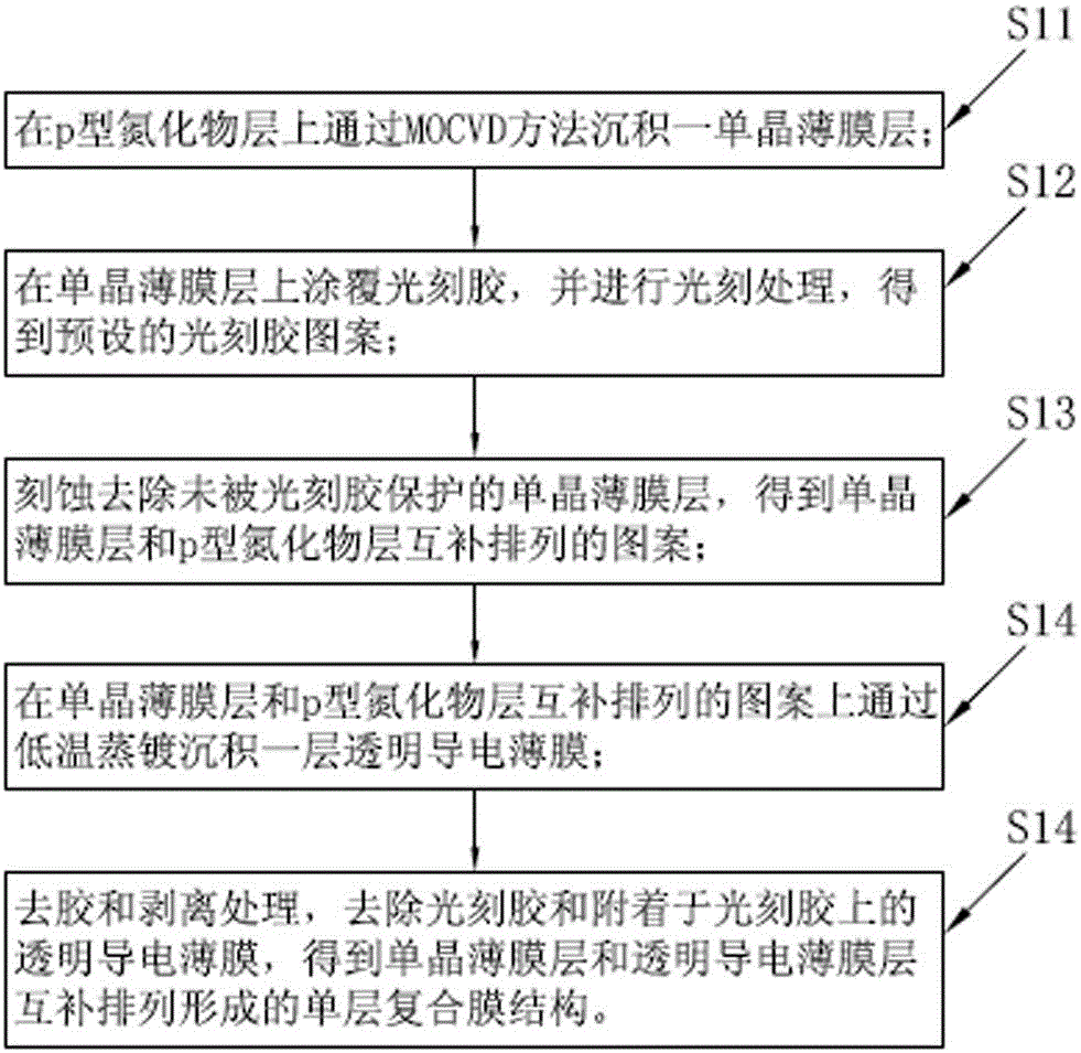
[0039] Please refer to figure 2 Shown, the present invention also provides a kind of preparation method of current spreading electrode, and described method comprises the following steps:

[0040] S11. Depositing a single crystal thin film layer on the p-type nitride layer by MOCVD method;

[0041] S12. Coating photoresist on the single crystal thin film layer and performing photolithography treatment to obtain a preset photoresist pattern;

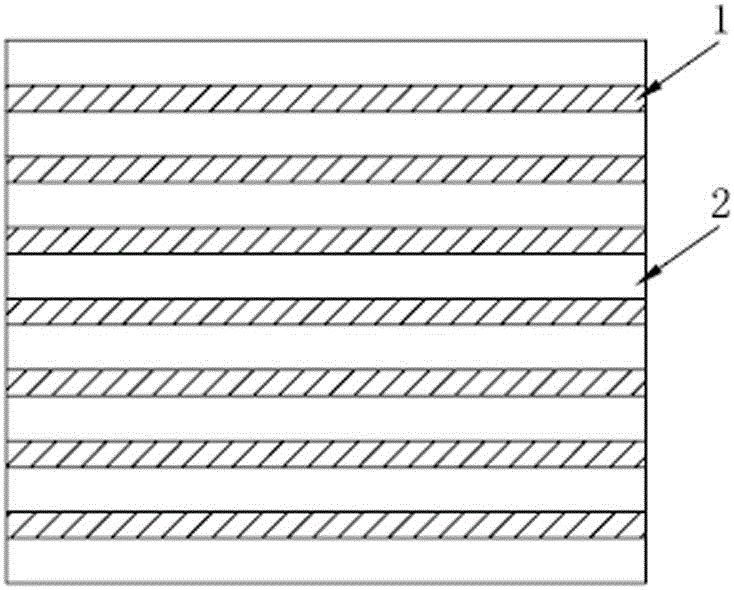
[0042] S13. Etching and removing the single crystal thin film layer not protected by the photoresist to obtain a complementary arrangement pattern of the single crystal thin film layer and the p-type nitride layer;

[0043] S14. Depositing a layer of transparent conductive film by low-temperature evaporation on the pattern in which the single crystal thin film layer and the p-type nitride layer are complementary arranged;

[0044] S15 , stripping and stripping, removing the photoresist and the transparent conductive film attached to th...


PUM

PropertyMeasurementUnit
refractive indexaaaaaaaaaa

Abstract

The invention provides a current diffusion electrode, which comprises single crystal film layers and transparent conductive film layers. The single crystal film layers and the transparent conductive film layers are arranged in a complementary manner so as to form a single-layer composite film; the single-layer composite film can be in contact with a p-type nitride layer; and the single crystal film layers are made of transparent conductive oxide. The invention also provides a method for manufacturing the current diffusion electrode, a semiconductor emitting device with the current diffusion electrode, and a method for manufacturing the semiconductor emitting device. The single crystal film layers and the transparent conductive film layers are arranged in the complementary manner so as to form the single-layer composite film; the single-layer composite film can be in contact with the p-type nitride layer; if the single crystal film layers are in contact with a p-type nitride semiconductor, ohmic contact is easy to form, contact resistance is low, current diffusion is uniform, and electric properties of a nitride semiconductor device are improved; and besides, light transmission of the transparent conductive film layers is good, light penetration rate and light emergent efficiency of the transparent conductive film layers are high, and optical properties of the nitride semiconductor device are improved.

Description

technical field [0001] The invention belongs to the field of semiconductors, and in particular relates to a current diffusion electrode, a preparation method and a semiconductor light emitting device. Background technique [0002] As wide bandgap materials, group III nitride materials such as gallium nitride (GaN), aluminum gallium nitride (GaAlN), indium gallium nitride (InGaN) and aluminum indium gallium nitride (InAlGaN) have high thermal conductivity, high dielectric Excellent characteristics such as electric constant, high electron saturation migration rate and high chemical stability, these characteristics make this series of materials have great application prospects in short-wavelength light-emitting devices, ultraviolet detectors, high-power microwave devices and high-temperature resistant electronic devices. . [0003] Since the high doping of p-type GaN has not been able to effectively break through, and there is no metal with a work function greater than the wor...

Claims


Application Information

Patent Timeline
Patent Type & Authority Patents(China)
IPC IPC(8): H01L33/36H01L33/42H01L33/00
Inventor 张戈
Owner BYD SEMICON CO LTD
Why Eureka
Try Eureka