
Integrated method for operating temperature controllable multi-chip modules

A technology of multi-chip components and integration methods, applied in electrical components, electrical solid-state devices, semiconductor devices, etc., can solve problems such as heat conduction, achieve stable and reliable work, improve long-term reliability, and broad market prospects.

Inactive Publication Date: 2016-01-20
GUIZHOU ZHENHUA FENGGUANG SEMICON
View PDF5 Cites 0 Cited by
  • Summary
  • Abstract
  • Description
  • Claims
  • Application Information

AI Technical Summary

Problems solved by technology

[0005] The purpose of the present invention is to provide an integration method of a temperature-controllable multi-chip module to solve the technical problems of internal heat conduction and internal working temperature control of the MCM multi-chip module package, which can ensure the temperature stability of the long-term operation of the device and improve the performance of the device. long-term reliability

Method used


Image

  • Integrated method for operating temperature controllable multi-chip modules
  • Integrated method for operating temperature controllable multi-chip modules
  • Integrated method for operating temperature controllable multi-chip modules

Examples


Embodiment 1

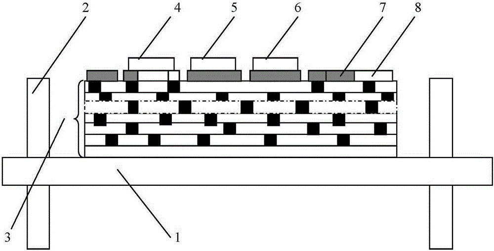
[0017] Embodiment 1: the original integrated process such as Figure 4 As shown, the process is briefly described as follows:

[0018] (1) Casting: By changing the material type and ratio, the substrate with expected design requirements (such as thermal conductivity, dielectric constant, loss factor, insulation resistance, breakdown voltage, etc.) can be obtained. According to the design requirements, the proportioning of the slurry is completed, and the slurry is cast on the tape casting machine along the substrate film into a thin sheet; at this time, it becomes a raw porcelain material, which is rolled into a roll after pre-drying, and is ready for use;

[0019] ⑵Cutting piece: The surface inspection of the rolled green ceramic sheet after casting is carried out and cut into ceramic blocks of specified size, that is, block blocks;

[0020] (3) Punching: In order to make the interconnection structure of each layer of LTCC, it is necessary to punch through holes or positioni...

Embodiment 2

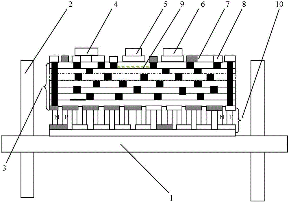
[0035] Embodiment 2 The technological process of the present invention is as Figure 5 Shown; The present invention, on the basis of original flow process, increases thick-film thermistor slurry screen printing and sintering, LTCC substrate back side thick-film conductor slurry screen printing and solidification, the preparation and processing of TEC substrate ceramic substrate The printing and sintering of thick film conduction tape, the preparation of N-type and P-type semiconductor grains required by TEC, the integration of PTCC and TEC, etc. The overall process flow is briefly described as follows:

[0036] (1) Casting: By changing the material type and ratio, the substrate with design requirements (such as thermal conductivity, dielectric constant, loss factor, insulation resistance, breakdown voltage, etc.) can be obtained. According to the design requirements, the proportioning of the slurry is completed, and the slurry is cast on the tape casting machine along the subs...


PUM


Abstract

The invention discloses an integrating method of a working temperature controllable multi-chip component. Integrating technology of a thermal signal-acquiring thick film thermistor, micro thermoelectric refrigeration, thick film screen printing, thick film laser resistor trimming, and co-sintering ceramic at low temperature in multiple layers, is adopted by the method, wherein a multi-layer co-sintered ceramic substrate is formed by sintering multiple layers of ceramic, and each layer comprises a metalized through hole, a conduction band and a stop band; the thick film thermistor is buried in the second layer of a ceramic plate of the multi-layer co-sintered ceramic substrate, and the burying position faces an integrated circuit chip which is sensitive to temperature; the conduction band, the stop band, the integrated circuit chip, a small-capacity inducer and a micro element are integrated on the front surface of the substrate; and a semiconductor cooler is integrated on the back surface of the substrate and is respectively connected to a surface bonding area through the through hole from the two ends of an N type semiconductor and a P type semiconductor. By the component, devices work in a specific working temperature range for a long time, the temperature stability for long-term work of the devices can be ensured, and the long-term reliability of the devices is improved.

Description

technical field [0001] The present invention relates to a multi-chip module (abbreviated as MCM), more specifically, to a thick-film multilayer low-temperature co-fired ceramic multi-chip module (abbreviated as MCM-C), especially to a thick-film multilayer low-temperature co-fired ceramic multi-chip with controllable operating temperature components. Background technique [0002] A device that mounts multiple semiconductor chips in the same package is a multi-chip module. In the original multi-chip component integration technology, the thick-film low-temperature multi-layer co-fired ceramic (LTCC for short) substrate is directly mounted on the base of the shell, and then the thick-film conductive paste is screen-printed and sintered on the LTCC substrate. Material or thick film resistor paste, laser trimming of sintered thick film resistors, mounting semiconductor chips, chip components, and then bonding with bonding wire (gold wire or silicon aluminum wire) to complete the...

Claims


Application Information

Patent Timeline
Patent Type & Authority Patents(China)
IPC IPC(8): H01L21/50H01L21/48H01L23/15
Inventor 杨成刚苏贵东刘俊
Owner GUIZHOU ZHENHUA FENGGUANG SEMICON
Learn More