Method for improving electrical interconnection characteristic of carbon nano tube

A technology of carbon nanotubes and electrical characteristics, applied in nanotechnology, nanotechnology, nanotechnology for information processing, etc., can solve the problems of low space occupancy rate of carbon nanotubes, excessive resistance, etc., and achieve improved interconnection electrical The effect of the characteristic

Active Publication Date: 2013-01-16
TIANJIN UNIVERSITY OF TECHNOLOGY
View PDF7 Cites 6 Cited by
  • Summary
  • Abstract
  • Description
  • Claims
  • Application Information

AI Technical Summary

Problems solved by technology

[0006] The purpose of the invention is to solve the problem of contact between carbon nanotubes and metals, and the problem of excessive resistance caused by the low space occupancy rate of carbon nanotubes, and proposes a method for improving the electrical characteristics of carbon nanotube interconnections

Method used


Image

  • Method for improving electrical interconnection characteristic of carbon nano tube
  • Method for improving electrical interconnection characteristic of carbon nano tube
  • Method for improving electrical interconnection characteristic of carbon nano tube

Examples


Embodiment 1

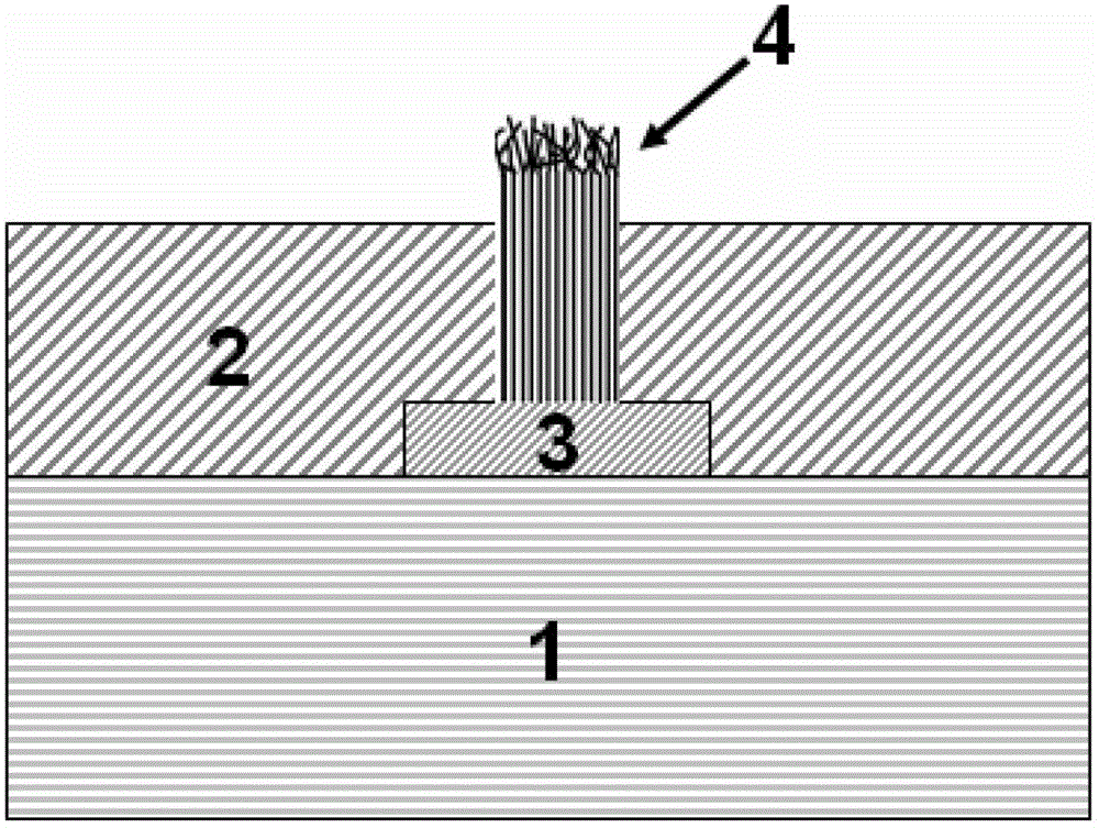
[0043] Combined with a mask plate and a photolithography machine, a layer of high-purity aluminum 2 with a thickness of about 500 nm is sputtered on the silicon substrate 1 by magnetron sputtering as the bottom electrode. Then a silicon dioxide dielectric layer 3 with a uniform thickness is deposited on the lower electrode, and the thickness of the silicon dioxide is 3 μm. Afterwards, photolithography and BOE wet etching are used to etch a via hole above the dielectric layer corresponding to the lower electrode. The diameter of the via hole is 1 μm, and the etching stops after reaching the lower electrode.

[0044] A layer of iron with a thickness of 5 nm was deposited as a catalyst in the vias by ion beam sputtering. And use plasma-enhanced chemical vapor deposition system to grow carbon nanotubes 4 . A mixture of hydrogen and acetylene (the ratio of the two is about 1:3) is passed into the chamber, the pressure is about 900Pa, the temperature is between 500-700°C, and the g...

Embodiment 2

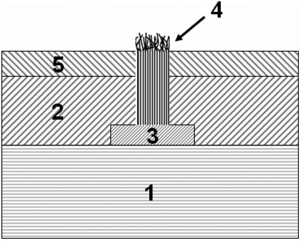
[0051] A bottom electrode pattern is prepared on the silicon base 1 by using a photolithography method in combination with a mask plate. Afterwards, a layer of high-purity silver 2 with a thickness of about 300 nm is deposited as the bottom electrode by electron beam evaporation. Then, a layer of silicon dioxide dielectric layer 3 with a uniform thickness was deposited on the bottom electrode by plasma enhanced chemical vapor deposition, and the thickness of the silicon dioxide was 5 μm. Afterwards, photolithography combined with dry etching is used to etch a via hole above the dielectric layer corresponding to the lower electrode. The diameter of the via hole is 2 μm, and the etching stops after reaching the lower electrode.

[0052] A layer of iron-nickel alloy with a thickness of 5nm was deposited as a catalyst in the through hole by ion beam sputtering. And use plasma-enhanced chemical vapor deposition system to grow carbon nanotubes 4 . A mixed gas of hydrogen and metha...

Embodiment 3

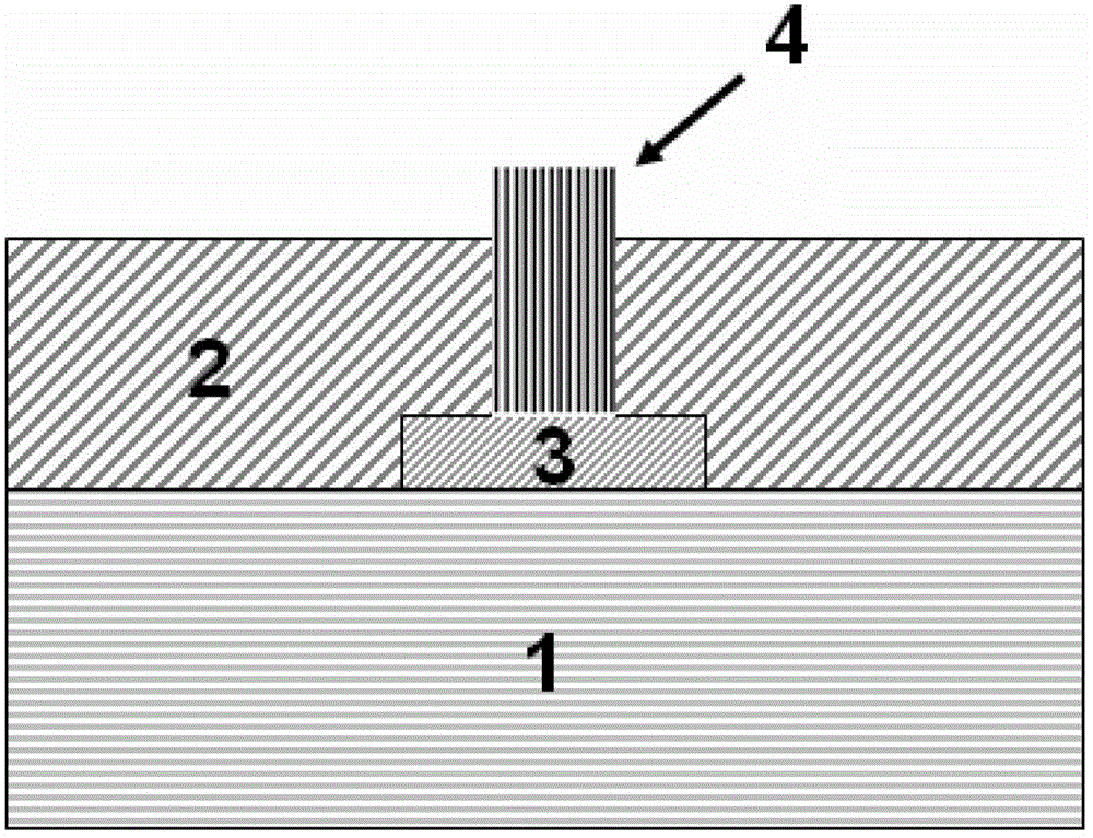
[0059] A bottom electrode pattern is prepared on the silicon substrate 1 by combining a mask plate and using a photolithography method. Then magnetron sputtering is used to deposit a layer of high-purity silver platinum with a thickness of about 100 nm as the bottom electrode. Then, a layer of silicon dioxide dielectric layer 3 with a uniform thickness was deposited on the lower electrode by plasma enhanced chemical vapor deposition, and the thickness of the silicon dioxide was 7 μm. Thereafter, photolithography and reactive ion etching are used to etch a via hole above the dielectric layer corresponding to the lower electrode. The diameter of the via hole is 3 μm, and the etching stops after reaching the lower electrode.

[0060]A layer of cobalt with a thickness of 5nm was deposited as a catalyst in the through holes by atomic layer deposition. And use plasma-enhanced chemical vapor deposition system to grow carbon nanotubes 4 . A mixed gas of argon, hydrogen and acetylene...


PUM

PropertyMeasurementUnit
thicknessaaaaaaaaaa
thicknessaaaaaaaaaa
thicknessaaaaaaaaaa

Abstract

The invention provides a method for improving the electrical interconnection characteristic of a carbon nano tube. The problem of overlarge interconnection resistance brought by low space occupancy of the carbon nano tube is solved through a through hole filling technology. The method mainly comprises the following steps: the carbon nano tube is firstly grown in a prefabricated through hole, then a layer of photoresist is coated in a rotating mode on the whole surface, and high-temperature hardening treatment is carried out on the photoresist; then the whole structure is polished by a chemical mechanical polishing method, the surplus photoresist is removed with an organic solvent after polishing, metal is filled in the through hole, and chemical mechanical polishing is carried out again after filling; and finally an electrode is arranged on the top of the carbon nano tube to realize metallization contact. The method disclosed by the invention has the advantages that a method for fixing the carbon nano tube is provided, a gap of the carbon nano tube is filled with the metal more effectively, the contact resistance of the carbon nano tube and the metal is reduced, the whole process is compatible with the currently commonly used process of semiconductors, and the method is easy to realize.

Description

technical field [0001] The invention relates to the technical field of integrated circuit interconnection and the polishing field of carbon-based materials. In particular, a method for improving the electrical properties of carbon nanotube interconnects. technical background [0002] At present, in the integrated circuit industry, the commonly used interconnection materials are mostly metal materials, such as Cu, Al, W, etc., among which the Cu connection occupies a dominant position. However, with the sharp decrease of device size, Cu interconnection faces many problems. At present, semiconductor devices have been developed to the 22nm node, which is close to the physical limit of Cu. At this time, due to the intensification of Cu interconnection surface scattering and grain boundary scattering, its resistance increases significantly, thereby increasing the circuit. RC delay. ITRS predicts that when the IC enters the 32nm process node, the current density that the interc...

Claims


Application Information

Patent Timeline
Patent Type & Authority Applications(China)
IPC IPC(8): H01L21/768H01L21/28B82Y10/00
Inventor 张楷亮任君王芳冯玉林董莉兰馗博赵金石
Owner TIANJIN UNIVERSITY OF TECHNOLOGY
Why Eureka
Try Eureka