

Preparation method of addressable nano molecular junction
A nano-scale, molecular junction technology, applied in nanotechnology, nanotechnology, nanotechnology for information processing, etc., can solve problems such as complex devices, affecting nano-device research, and unstable molecular junctions, so as to prevent leakage and ensure Addressability, effects of enhanced adhesion
- Summary
- Abstract
- Description
- Claims
- Application Information
AI Technical Summary
Problems solved by technology
Method used
Image

Examples
example 1
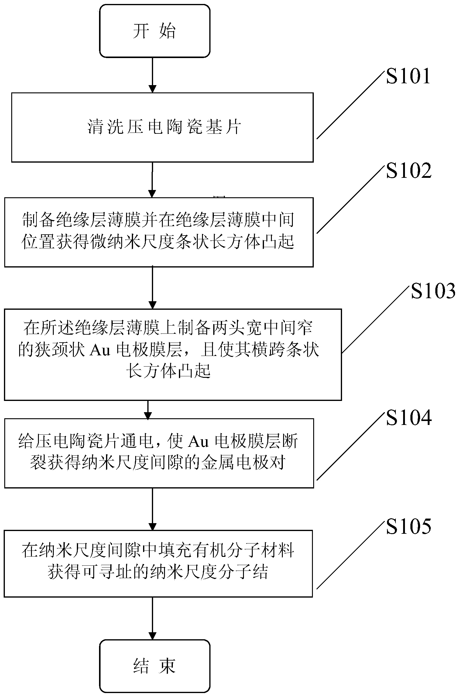
[0023] In step 101, the piezoelectric ceramic substrate is cleaned.
[0024] The piezoelectric strain constant is 2.25×10 -10 m / v P8-1 piezoelectric ceramics (lead zirconate titanate) as the substrate, immerse in acetone, absolute ethanol and deionized water for 5 to 8 minutes, respectively, and ultrasonically clean the remaining inorganic substances on the piezoelectric ceramic substrate And organic matter to ensure that it has a good charge transport ability, and let it dry naturally.
[0025] In step 102, a gate and a gate insulator are prepared.
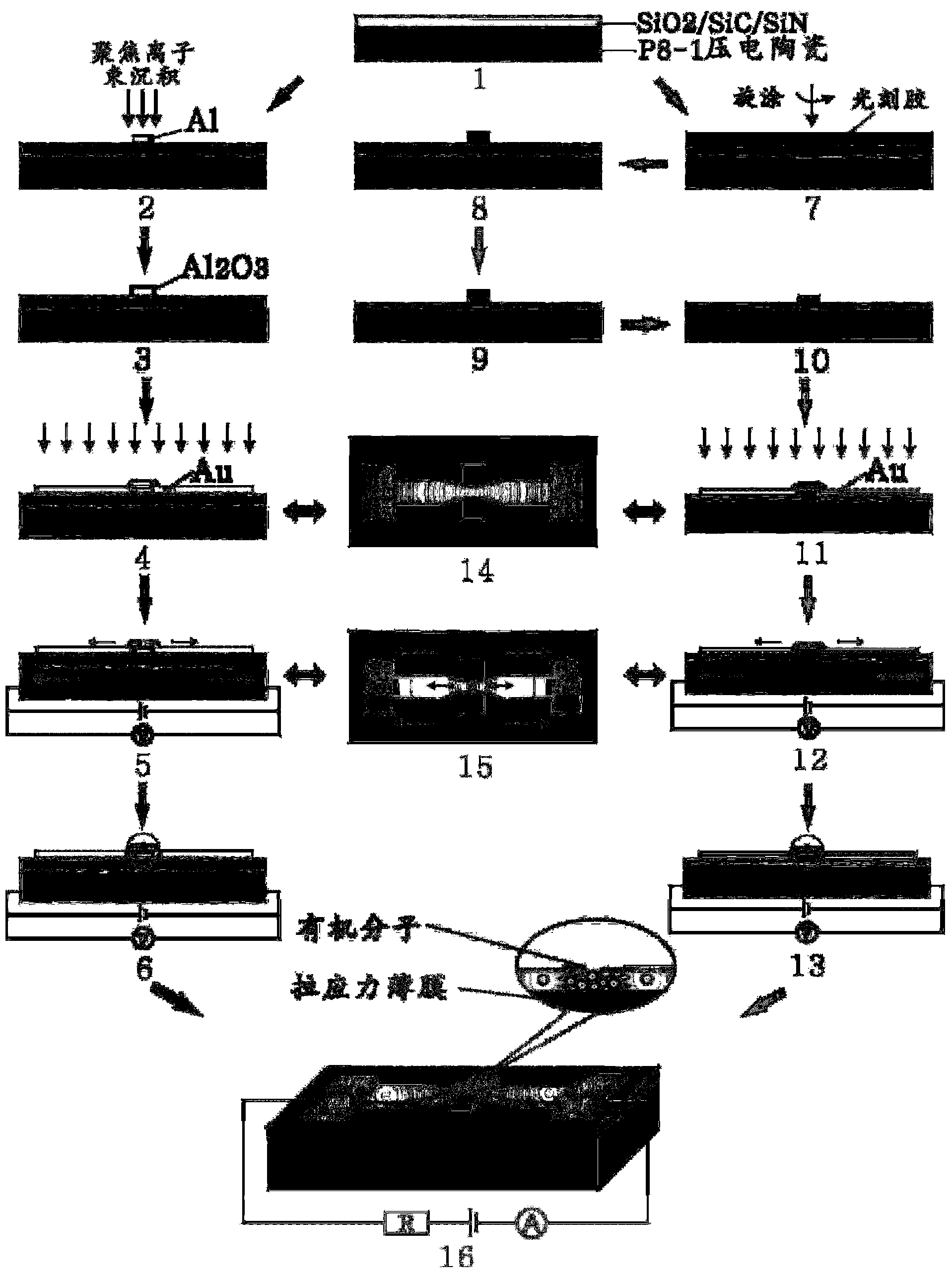
[0026] like figure 2 In the process shown in No. 1, before preparing the gate and gate insulator, a silicon oxide film with a thickness of 50-70 nm is deposited on the surface of the piezoelectric ceramic substrate by reactive magnetron sputtering, and single crystal silicon is used as the target material. Argon is used as the working gas, and oxygen is used as the reaction gas. The range of process parameters is: the volume ...
Embodiment 2
[0032] In step 101, the piezoelectric ceramic substrate is cleaned. The piezoelectric strain constant is 2.25×10 -10 m / v P8-1 piezoelectric ceramics (lead zirconate titanate) as the substrate, immerse in acetone, absolute ethanol and deionized water for 5 to 8 minutes, respectively, and ultrasonically clean the remaining inorganic substances on the piezoelectric ceramic substrate And organic matter to ensure that it has a good charge transport ability, and let it dry naturally.
[0033] In step 102, a silicon nitride film is prepared. like figure 2 In the process shown in No. 1, a silicon nitride film with a thickness of 50-70 nm is deposited on the surface of the piezoelectric ceramic substrate by plasma-enhanced chemical vapor deposition (PECVD). The range of process parameters is: the temperature of the piezoelectric ceramic substrate is 250 ~300℃, RF power 150~250W, reaction gas flow ratio m(SiH 4 ):m(NH 3 )=30:20mL / min, reaction pressure 2~5Pa. It can also be reali...
example 3
[0039] In step 101, the piezoelectric ceramic substrate is cleaned. The piezoelectric strain constant is 2.25×10 -10 m / v P8-1 piezoelectric ceramics (lead zirconate titanate) as the substrate, immerse in acetone, absolute ethanol and deionized water for 5 to 8 minutes, respectively, and ultrasonically clean the remaining inorganic substances on the piezoelectric ceramic substrate And organic matter to ensure that it has a good charge transport ability, and let it dry naturally.
[0040] In step 102, a silicon oxide film is prepared. like figure 2 In the process shown by the middle mark 1, a silicon oxide film with a thickness of 50-70nm is deposited on the surface of the piezoelectric ceramic substrate by reactive magnetron sputtering method, with single crystal silicon as the target material, argon as the working gas, oxygen As the reaction gas, the range of process parameters is: oxygen volume fraction 0-50%, reaction pressure 0.02-0.07Pa. It can also be obtained by PEC...
PUM
| Property | Measurement | Unit |
|---|---|---|
| thickness | aaaaa | aaaaa |
Abstract
Description
Claims
Application Information