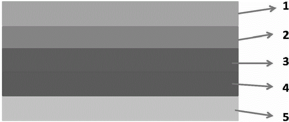
Solar cell back plate and solar cell
A solar cell and backplane technology, applied in the field of solar cells, can solve problems such as difficulty in blocking, detachment of the oxide layer, and reduction of the aging resistance of the backplane, and achieve enhanced aging resistance, excellent gas barrier performance, and good barrier properties. Gas effect
- Summary
- Abstract
- Description
- Claims
- Application Information
AI Technical Summary
Problems solved by technology
Method used
Image
Examples
preparation example Construction
[0040] The preparation method of the inorganic layer is not limited in the present invention, and may be a vapor phase deposition method or a liquid phase method well known to those skilled in the art, preferably a sputtering method or an ion plating method. In the present invention, the barrier layer is preferably prepared according to the following method: an inorganic film of silicon oxide is plated on an organic layer made of polyethylene naphthalate by an ion plating process to obtain a barrier layer.
[0041]The inorganic layer prepared by vapor phase deposition method or liquid phase method can be combined with the organic layer to form a barrier layer without a binder, and the inorganic oxide and / or inorganic nitride have anti-corrosion and anti-aging properties, not It will be corroded by external conditions such as high temperature and high humidity. The barrier layer obtained by compounding the inorganic layer and the organic layer with excellent gas barrier propert...
Embodiment 1
[0067] The weather-resistant layer and the barrier layer are bonded together by an adhesive layer. The bonding layer is made of polyurethane adhesive with a thickness of 10 μm; the weather-resistant layer is made of polyvinylidene fluoride with a thickness of 30 μm, and the weather-resistant layer is treated with surface corona to make its dyne value is 56; the barrier layer is obtained by compounding an organic layer and an inorganic layer, and the composite method is: through an evaporation process, an inorganic layer made of silicon oxide is evaporated on the organic layer to obtain a barrier layer, wherein the The organic layer is made of polyethylene naphthalate and has a thickness of 80 μm, and the thickness of the inorganic layer is 50 μm. The bonding layer is composited with the inorganic layer in the barrier layer.
[0068] Through the double-layer co-extrusion process, the organic layer in the barrier layer is combined with the structural reinforcement layer. The st...
Embodiment 2
[0071] The weather-resistant layer and the barrier layer are bonded together by an adhesive layer. The bonding layer is made of polyurethane adhesive with a thickness of 10 μm; the weather-resistant layer is made of polyvinylidene fluoride with a thickness of 30 μm, and the weather-resistant layer is treated with surface corona to make its dyne value is 56; the barrier layer is obtained by compounding an organic layer and an inorganic layer, and the composite method is: through an evaporation process, an inorganic layer made of silicon oxide is evaporated on the organic layer to obtain a barrier layer, wherein the The organic layer is made of polyethylene naphthalate and has a thickness of 80 μm, and the thickness of the inorganic layer is 30 μm. The bonding layer is composited with the inorganic layer in the barrier layer.
[0072] Through the double-layer co-extrusion process, the organic layer in the barrier layer is combined with the structural reinforcement layer. The st...
PUM
| Property | Measurement | Unit |
|---|---|---|
| Thickness | aaaaa | aaaaa |
| Thickness | aaaaa | aaaaa |
| Thickness | aaaaa | aaaaa |
Abstract
Description
Claims
Application Information

