

Chip structure for PCR (polymerase chain reaction) rapid reaction
A chip structure, rapid response technology, applied in specific-purpose bioreactor/fermenter, bioreactor/fermenter combination, biochemical instruments, etc., can solve the problems of rising processing cost, pollution, waste transfer of reagents, etc. Improved efficiency, high heating/cooling rate, cost saving effect
- Summary
- Abstract
- Description
- Claims
- Application Information
AI Technical Summary
Problems solved by technology
Method used
Image

Examples
Embodiment 1
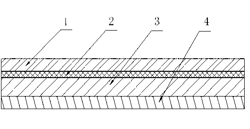
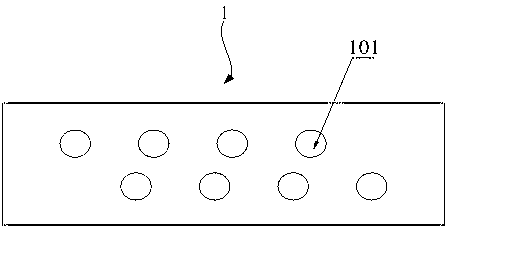
[0031]PCR chip: Quartz glass is used as the substrate, the size is 80mm×20mm, and the thickness is 2mm. Using laser drilling technology, two rows of microcavity holes are processed on the quartz glass sheet. Each row has eight microcavity holes of the same aperture. Among the rows of microcavity holes, the diameter of one row of microcavity holes is 1.6mm, the diameter of the other row of microcavity holes is 3.0mm, and the depth is 1.5mm. The distance between the centers of the microcavity holes is 9mm. The distance between the hole center and the long side is 8.5 mm, and the distance between the microcavity hole center and the short side is 5.5 mm. The processed quartz glass chip needs to be cleaned by ultrasonic waves. The process is as follows: wash in acetone solution for 5 minutes; take it out and put it in ethanol solution for 5 minutes, put it in deionized water after taking it out, wash it for 5 minutes, and blow dry with nitrogen.
[0032] Cover sheet: PC board mater...
Embodiment 2
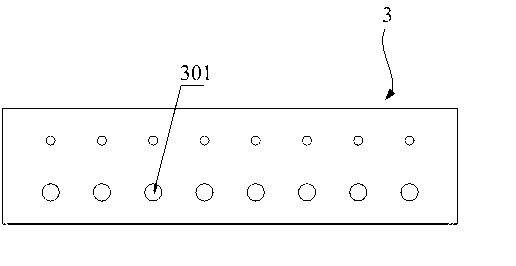
[0041] PCR chip: 7740 glass and silicon wafer are used as chip substrates. The 7740 glass has a diameter of 100mm and a thickness of 1.5mm. Two units of 80mm×20mm are drawn on the glass. Using the laser drilling process, each unit has two rows of microcavity holes as through holes, and each row contains eight microcavity holes with the same aperture. The diameters of the two rows of microcavity holes in the same unit are 1.6mm and 3.0mm, respectively. The distance between the centers of the microcavity holes is 9 mm, the distance between the center of the microcavity holes and the long side of the cell is 8.5 mm, and the distance between the center of the through hole and the short side of the cell is 5.5 mm. The silicon wafer has a diameter of 100 mm and a thickness of 500 μm. Using anodic bonding technology, the cleaned glass sheet and silicon sheet with through holes are bonded together to form a PCR chip. The processed glass and silicon wafers need to be cleaned by ultras...
PUM
| Property | Measurement | Unit |
|---|---|---|
| Length and width | aaaaa | aaaaa |
| Thickness | aaaaa | aaaaa |
Abstract
Description
Claims
Application Information