Semiconductor laser cavity surface passivation film structure and preparation method thereof

A passivation film and laser technology, which is applied in semiconductor lasers, lasers, laser components, etc., can solve the problems of expensive equipment, high equipment requirements, and complicated processes, and achieve simple preparation methods, low dielectric constant, and reduced stress. Effect

Inactive Publication Date: 2013-04-03
CHANGCHUN UNIV OF SCI & TECH
View PDF3 Cites 4 Cited by
  • Summary
  • Abstract
  • Description
  • Claims
  • Application Information

AI Technical Summary

Problems solved by technology

The practice that is often adopted in the world is to coat a layer of Si as a passivation barrier layer before plating the cavity mask, but the light band suitable for Si is narrow, and the light absorption is large, so for semiconductor lasers with shorter wavelengths, Si passivation The application of chemical technology has certain limitations
Moreover, in order to minimize the oxidation of the cavity surface, cleavage is usually carried out in an ultra-high vacuum, and a passivation layer and a cavity film are immediately plated. Although this method can better improve the reliability of the device, it requires more equipment. High, complex process, expensive equipment
In addition, ion beam evaporation of ZnSe and ZnS after ion cleaning on the cavity surface is also a good passivation method. However, ZnSe and ZnS are prone to deliquescence and instability in humid environments, which have certain limitations for the application of lasers in certain aspects. limitation

Method used


Image

  • Semiconductor laser cavity surface passivation film structure and preparation method thereof

Examples


Embodiment Construction

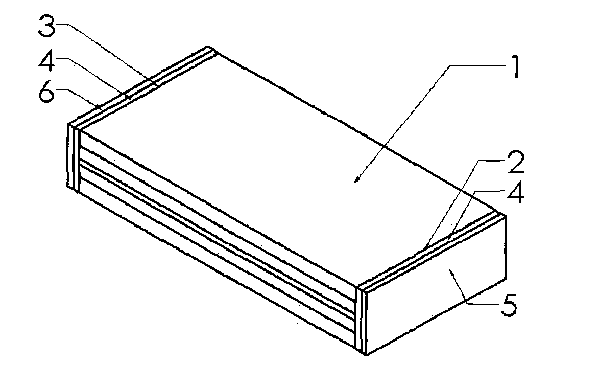
[0020] After the semiconductor laser is cleaved into bar 1 in the air, it is loaded into a special coating fixture, and then put into a magnetron sputtering vacuum chamber.

[0021] Ion pre-cleaning, that is, using low-energy large-beam ions with energy less than 100eV in the magnetron sputtering vacuum chamber to non-destructively remove oxides and impurities on the cavity surface cleaved in air, as well as the surface states and interface states formed by non-radiative recombination. In the center: carry out the ion pre-cleaning on the front cavity surface 2 of the semiconductor laser for 30 seconds to 6 minutes.

[0022] In the high vacuum chamber of the magnetron sputtering system, the background vacuum is 3*10 -9 Torr, the deposition pressure is 16~20mTorr, h-BN is used as the target material, the substrate is equipped with a high-frequency AC power bias device to control the bombardment of the particles on the substrate, the substrate bias is -10~-120V; the RF power is 1...


PUM


Abstract

The invention relates to the technical field of semiconductor photoelectronic devices, in particular to a semiconductor laser cavity surface passivation film structure and a preparation method thereof. The semiconductor laser cavity prepares a cubic boron nitride (c-BN) film layer to serve as a passivation film of a laser cavity face, effectively reduces catastrophe optical damage of the laser cavity face, and improves reliability and stability of a laser device. After ion prewashing is conducted on the front cavity face and the back cavity face of a semiconductor laser bar, a magnetron sputtering method is adopted to deposit a cubic boron nitride (c-BN) layer on the front cavity face and the back cavity face of the bar, and then an anti-reflection film and a high-reflection film are respectively plated on the front cavity face and the back cavity face. The structure and the method can be applied to various semiconductor lasers.

Description

technical field [0001] The invention relates to the technical field of semiconductor optoelectronic devices, in particular to a semiconductor laser cavity surface passivation film structure and a preparation method thereof. technical background [0002] Semiconductor lasers are core devices in the fields of optical communication, optical pumping, and optical storage. Due to the influence of the interface state, impurity contamination or strain on the cavity surface, the light absorption is enhanced, and the temperature is sharply increased. The temperature increase further deteriorates the interface and enhances the light absorption. It is easy to oxidize and generate defects, which makes the laser performance occur. Attenuation and optical catastrophic damage, which is particularly prominent for high-power lasers. In order to reduce the influence of this factor and improve the reliability of laser devices, the laser cavity surface is usually coated. Generally, this coating...

Claims


Application Information

Patent Timeline
IPC IPC(8): H01S5/028C23C14/06C23C14/35
Inventor 芦鹏郭仁红刘学东赵英杰许鹏李再金王勇李特乔忠良刘国军马晓辉
Owner CHANGCHUN UNIV OF SCI & TECH
Why Eureka
Try Eureka