Light emitting diode (LED) epitaxial wafer with N type insertion layer with trapezoidal structure and growth method thereof

A technology of LED epitaxial wafer and trapezoidal structure, which is applied in the direction of electrical components, circuits, semiconductor devices, etc., can solve the problems of enhanced vertical confinement and reduced electron quantity, and achieve the effects of avoiding confinement, improving crystal quality and promoting lateral movement of electrons

Active Publication Date: 2013-06-19
宁波安芯美半导体有限公司
View PDF3 Cites 15 Cited by
  • Summary
  • Abstract
  • Description
  • Claims
  • Application Information

AI Technical Summary

Problems solved by technology

Although the large polarization difference at the heterointerface between the N-type AlGaN layer and the N-type GaN layer will induce a high concentration of two-dimensional electron gas and promote the lateral movement of electrons, the longitudinal confinement effect of the two-dimensional electron gas on carriers It is also enhanced, so that electrons gather at the heterointerface, resulting in a reduction in the number of electrons migrating to the quantum well region, so the two-dimensional electron gas structure is a double-edged sword

Method used


Image

  • Light emitting diode (LED) epitaxial wafer with N type insertion layer with trapezoidal structure and growth method thereof
  • Light emitting diode (LED) epitaxial wafer with N type insertion layer with trapezoidal structure and growth method thereof

Examples


Embodiment 1

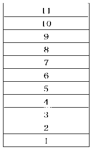
[0024] Such as figure 1 The shown LED epitaxial wafer structure includes, from bottom to top, substrate 1, low-temperature GaN buffer layer 2, GaN undoped layer 3, first N-type GaN layer 4, N-type AlGaN insertion layer 5, second N-type GaN layer 6 , multiple quantum well layer 7 , low-temperature P-type GaN layer 8 , P-type AlGaN layer 9 , high-temperature P-type GaN layer 10 , and P-type contact layer 11 .

[0025] In this example, high-purity hydrogen (H2) or nitrogen (N2) is used as carrier gas, trimethylgallium (TMGa), triethylgallium (TEGa), trimethylaluminum (TMAl), trimethylindium (TMIn ) and ammonia (NH3) as sources of Ga, Al, In, and N, respectively, and silane (SiH4) and magnesocene (CP2Mg) as N and P-type dopants, respectively.

[0026] The method for growing a GaN-based LED epitaxial structure with an N-type insertion layer of a trapezoidal structure in this embodiment includes the following specific steps:

[0027] Step 1: Clean the substrate 1 at a high tempera...


PUM


Abstract

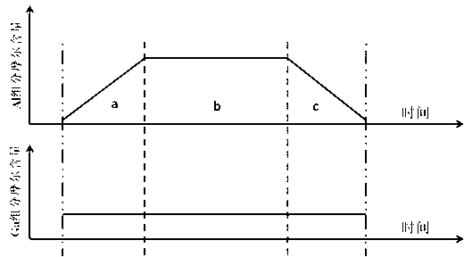
The invention discloses a light emitting diode (LED) epitaxial wafer with an N type insertion layer with a trapezoidal structure and a growth method thereof. The LED epitaxial wafer comprises a substrate, a low-temperature GaN buffer layer, a GaN non-doping layer, a first N type GaN layer, an N type AlGaN insertion layer, a second N type GaN layer, a multi-quantum well layer, a low-temperature P type GaN layer, a P type AlGaN layer, a high-temperature P type GaN layer and a P type contact layer sequentially from bottom to top, wherein the N type AlGaN insertion layer has a trapezoidal structure. According to the LED epitaxial wafer, the N type AlGaN insertion layer which consists of N type AlGaN layers (a, b and c) is grown on the first N type GaN layer; and the content of mole components of Ga in the N type AlGaN layers (a, b and c) is constant, and the content of mole components of Al is increased gradually, constant and reduced gradually. According to the LED epitaxial wafer, the N type AlGaN layer with the trapezoidal structure is inserted into the N type GaN layers, so that the dislocation density of a quantum well area is reduced effectively, the influence on the longitudinal migration of electrons due to the introduction of the N type AlGaN layer is reduced, and the luminous efficiency of gallium nitride-base LEDs is improved.

Description

technical field [0001] The invention belongs to the technical field of preparation of group III nitride materials, in particular to an LED epitaxial wafer with an N-type insertion layer of a trapezoidal structure and a growth method thereof. Background technique [0002] Light Emitting Diode (LED, Light Emitting Diode) is a semiconductor solid-state light-emitting device, which uses a semiconductor PN junction as a light-emitting material, and can directly convert electricity into light. Group III nitrides represented by gallium nitride are wide-bandgap semiconductor materials with direct bandgap, which have excellent properties such as high electron drift saturation velocity, good thermal conductivity, strong chemical bond, high temperature resistance and corrosion resistance. Its ternary alloy indium gallium nitride (InGaN) band gap is continuously adjustable from 0.7eV indium nitride (InN) to 3.4eV gallium nitride (GaN), and the emission wavelength covers the entire regio...

Claims


Application Information

Patent Timeline
Patent Type & Authority Applications(China)
IPC IPC(8): H01L33/14H01L33/20H01L33/00
Inventor 李刚郭丽彬蒋利民
Owner 宁波安芯美半导体有限公司
Why Eureka
Try Eureka