Method for preparing graphene nanopore array through chemical vapor deposition by using porous anodic alumina (PAA) as template

A graphene nanopore and alumina template technology, applied in the field of low-dimensional materials and new materials, can solve the problems of uneven distribution of holes, low yield, high hardware equipment requirements, etc., and achieve the effect of excellent controllability

Active Publication Date: 2013-08-14
SHANGHAI INST OF MICROSYSTEM & INFORMATION TECH CHINESE ACAD OF SCI
View PDF2 Cites 27 Cited by
  • Summary
  • Abstract
  • Description
  • Claims
  • Application Information

AI Technical Summary

Problems solved by technology

Chemical methods are relatively cheap, but not suitable for CVD-prepared graphene films because the pore density and pore distribution cannot be controlled
Similarly, the distribution of holes obtained by bombardment of atoms or ions is uneven, and high-resolution transmission electron microscopy shows that bombardment fragments will accumulate on the surface of the sample
In contrast, atomic force microscopy and focused ion beam technology can precisely control the position and even the size of the hole, but it requires high hardware equipment and the yield is very low

Method used


Image

  • Method for preparing graphene nanopore array through chemical vapor deposition by using porous anodic alumina (PAA) as template
  • Method for preparing graphene nanopore array through chemical vapor deposition by using porous anodic alumina (PAA) as template
  • Method for preparing graphene nanopore array through chemical vapor deposition by using porous anodic alumina (PAA) as template

Examples


preparation example Construction

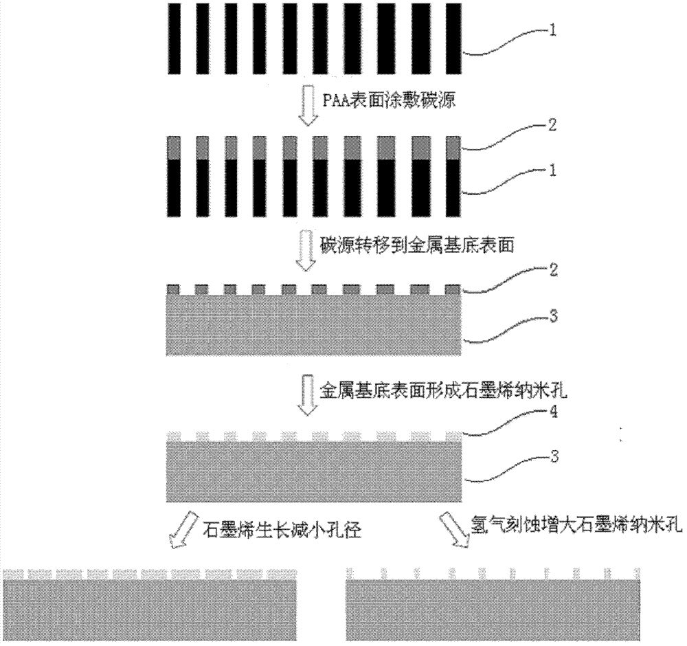
[0037] figure 1 It is a schematic flow chart of the preparation method of the present invention, in which 1 is a schematic cross-sectional view of a PAA template, 2 is a carbon source coated on the surface of PAA, 3 is a metal substrate, and 4 is a graphene nanopore formed on the surface of a metal substrate. Such as figure 1 Shown, the present invention adopts the porous anodic aluminum oxide (PAA) obtained by said method as template, has prepared graphene nanohole array, specifically comprises the steps:

[0038] 1) Coating the carbon source solution on the surface of PAA;

[0039] 2) Press the PAA template coated with the carbon source obtained in step 1) on the surface of the metal substrate, peel off the PAA template, keep the carbon source on the surface of the metal substrate and keep the carbon source on the surface of the PAA template Consistent patterns, forming a patterned distribution of carbon sources on the metal surface;

[0040] 3) annealing the metal substr...

Embodiment 1

[0045] Embodiment 1: the preparation of the graphene nanohole array that aperture is 10-90nm

[0046] The first step: prepare PAA template and copper substrate treatment, and apply carbon source on the surface of PAA. The aluminum sheet with a purity of 99.999% is mechanically and electrochemically polished to make the surface smooth; 0.3M oxalic acid aqueous solution is used as the electrolyte, the temperature of the electrolyte is 0°C, the electrolysis voltage is 40V, and the electrolysis is performed for 1 hour; Immerse the oxide layer in a phosphochromic acid solution at 60°C for 1 hour to remove the oxide layer; use the same process to perform secondary electrolysis to obtain a PAA template with a pore diameter of about 40nm and a pore wall of about 60nm. The atomic force microscope and field emission scanning electron microscope test results Such as Figure 4 and 5 shown. The copper sheet with a purity of 99.9% is mechanically and electrochemically polished to make th...

Embodiment 2

[0051] Embodiment 2: a graphene nanohole array with an aperture of 1-10 nanometers

[0052] The first step: similar to the first step in Example 1, the difference is that the voltage of the primary and secondary electrolysis of aluminum is 10V, the PAA pore diameter obtained is 10nm, and the pore wall is 10nm, and the difference is that the carbon source used is naphthalene.

[0053] The second step: the same as the second step in Example 1.

[0054] The third step: the substrate with the carbon source pattern is heated up to 1000° C. in a mixed gas of hydrogen and argon for heat treatment. Wherein: the hydrogen flow rate is 10 sccm, the argon flow rate is 200 sccm, and the temperature is kept for 30 minutes. The surface atomic force microscope photos and the field emission scanning electron microscope photos show that the graphene nanohole array is obtained, and the pore size is about 10nm.

[0055] Step 4: On the basis of the sample obtained in the third step, 2 sccm of m...


PUM

PropertyMeasurementUnit
pore sizeaaaaaaaaaa
pore sizeaaaaaaaaaa
pore sizeaaaaaaaaaa

Abstract

The invention provides a method for preparing a graphene nanopore array, which comprises the following steps: 1) coating a carbon source solution on the surface of a porous anodic alumina (PAA) template; 2) pressing the PAA template with the carbon source coated on the surface (obtained in the step 1)) on the surface of a metal base, peeling the PAA template, and ensuring that the carbon source is reserved on the surface of the metal base and the carbon source reserves a pattern which is consistent with that on the surface of the PAA template; and 3) performing annealing treatment on the obtained metal base in the presence of a mixed gas flow of hydrogen gas and argon gas, thus converting the carbon source into the graphene nanopore array. The nanopore array obtained by the invention is an interconnected nanopore array structure rather other a single nanopore or several nanopores; and the pore size of the nanopores can be regulated through the template effect of the PAA itself, and can be further regulated through growing and etching in the later stage. Thus, the pore size controllability is very excellent.

Description

technical field [0001] The invention relates to a method for preparing a graphene nanohole array, belongs to the field of low-dimensional materials and new materials, and is mainly applied to new graphene electronic devices. Background technique [0002] Graphene nanopores refer to the distribution of nanopores on a continuous two-dimensional graphene film. The diameter of the pores ranges from a few carbon atoms to tens of nanometers. Graphene nanopores with several nanometer diameters can be used for DNA detection and sorting (C.A.Merchant et al., DNA translocation through graphene nanopores, Nano Lett.10, 2010, 2915-2921), and smaller graphene nanopore structures can Used for selective separation of gas molecules (H.L.Du et al., Separation of hydrogen and nitrogen gases with porous graphene membrane, J.Phys.Chem.C, 115, 2011, 23261-23266), etc. In addition to the use of channels, the walls of adjacent graphene nanopores in the graphene nanopore array structure are equiv...

Claims


Application Information

Patent Timeline
Patent Type & Authority Applications(China)
IPC IPC(8): C01B31/04C01B32/186
Inventor 丁古巧谢晓明江绵恒
Owner SHANGHAI INST OF MICROSYSTEM & INFORMATION TECH CHINESE ACAD OF SCI
Why Eureka
Try Eureka