
Dielectric layer for embedded capacitance material, embedded capacitance material, preparation method and use of embedded capacitance material

A technology of dielectric layer and thin film layer, which is applied in the direction of circuit substrate materials, chemical instruments and methods, lamination, etc., can solve the problem of not being able to further increase the dielectric constant of buried capacitance materials, and the brittleness of buried capacitance materials ( Intensity, low dielectric constant of embedding materials and other issues, to achieve the effect of preventing leakage current, excellent strength and impact resistance, and improving the dielectric constant

Active Publication Date: 2013-10-23
GUANGDONG SHENGYI SCI TECH
View PDF9 Cites 12 Cited by
  • Summary
  • Abstract
  • Description
  • Claims
  • Application Information

AI Technical Summary

Problems solved by technology

[0010] The U.S. patent application US6693793 discloses a heat-resistant organic film as a support material in the middle, although it solves the problem of the strength of the embedding material (that is, solves the brittleness), but because the organic film with a low dielectric constant is used as the intermediate interlayer, The dielectric constant of the obtained embedding material is not high
[0011] Chinese patent CN102285168A uses a porous organic film and a ceramic filler compound as an intermediate layer to make an embedding material. Although it solves the problems of strength and toughness, it cannot further increase the dielectric constant of the embedding material to a greater extent.
However, this patent does not solve the problem of brittleness (poor strength) of the embedding material caused by the addition of conductive powder and a large amount of ceramic fillers
[0013] In view of the above problems, the present invention proposes a method that can not only improve the strength of the embedding material, but also greatly increase the dielectric constant of the embedding material, and prevent the increase of leakage current.

Method used


Image

  • Dielectric layer for embedded capacitance material, embedded capacitance material, preparation method and use of embedded capacitance material
  • Dielectric layer for embedded capacitance material, embedded capacitance material, preparation method and use of embedded capacitance material

Examples


Embodiment 1

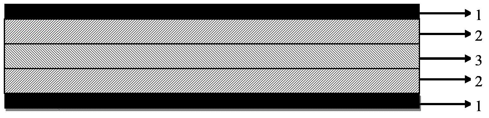
[0047] Dissolve 35g of bisphenol A type epoxy resin (epoxy resin A), 45g of brominated epoxy resin (epoxy resin B) and 20g of carboxy-terminated nitrile rubber (C) in ethylene glycol methyl ether, and add O-cresol novolac resin and 2-MI (2-methylimidazole) in a molar ratio of 0.9 to epoxy resin were mixed at room temperature to obtain a glue solution. The obtained glue solution was coated on the copper foil, and then baked in an oven at 155° C. for 5 minutes to be cured into stage B to obtain a resin-coated copper foil (RCC). The thickness of the RCC glue layer was 8 μm.

[0048] Dissolve 130g bisphenol A type epoxy resin (epoxy resin A), 70g brominated epoxy resin (epoxy resin B) and 500g carboxy-terminated nitrile rubber (C) in ethylene glycol methyl ether, then add Relative to the o-cresol novolac resin and 2-MI (2-methylimidazole) with a molar ratio of 0.9 to the epoxy resin, 300g of copper powder coated with barium titanate ceramic filler is added, and the particle size o...

Embodiment 2

[0051] 45g bisphenol A epoxy resin, 55g brominated epoxy resin and 20g phenoxy resin are dissolved in ethylene glycol methyl ether, and add o-cresol novolac resin and 2 -MI (2-methylimidazole), and then add 90.5g of barium titanate with a median particle size of 10nm, and its volume percentage is 15%, and then mix at room temperature to obtain a glue solution. The obtained glue solution was coated on the copper foil, and then baked in an oven at 155° C. for 5 minutes to be cured into stage B to obtain a resin-coated copper foil (RCC). The thickness of the RCC glue layer was 13 μm.

[0052] Dissolve 250g of polyimide resin and 150g of hydroxyl-terminated nitrile rubber in ethylene glycol methyl ether, then add 125g of bisphenol A epoxy resin and 75g of BT resin, and then add silver powder coated with barium titanate ceramic filler 400g, the median particle diameter of silver powder is 100nm, then mixed at room temperature to obtain glue. The obtained glue solution was coated o...

Embodiment 3

[0055] Dissolve 45g bisphenol A type cyanate resin (resin A), 55g brominated epoxy resin (epoxy resin B) and 20g carboxy-terminated nitrile rubber (C) in ethylene glycol methyl ether, and add 2 -MI (2-methylimidazole), and then add 342g of barium titanate with a median particle size of 100nm, the volume fraction of which is 40%, and mix at room temperature to obtain a glue solution. The obtained glue solution was coated on the copper foil, and then baked in an oven at 155° C. for 5 minutes to be cured to stage B to obtain a resin-coated copper foil (RCC). The thickness of the RCC glue layer was 25 μm.

[0056] Dissolve 95g bisphenol A type cyanate resin (resin A), 55g brominated epoxy resin (epoxy resin B) and 400g carboxy-terminated nitrile rubber (C) in ethylene glycol methyl ether, then add 2 -MI (2-methylimidazole), then add 450g of nickel powder coated with barium titanate ceramic filler, the median particle size of the nickel powder is 300nm, and then mix at room tempera...


PUM

PropertyMeasurementUnit
thicknessaaaaaaaaaa
thicknessaaaaaaaaaa
particle sizeaaaaaaaaaa

Abstract

The invention relates to a dielectric layer for an embedded capacitance material and the embedded capacitance material. The dielectric layer is composed of a thin film layer with good flexibility and resin composition layers respectively arranged at the upper side and the lower side of the thin film layer. The thin film layer contains a conductive powder coated with a ceramic packing, and is prepared by the conductive powder coated with the ceramic packing and a resin composition. The embedded capacitance material provided by the invention has low tensile modulus, high elongation rate, excellent strength and excellent impact resistance, and prevents a fragmentation phenomenon from appearing during a double-sided etching process or a drilling process of a circuit board; and at the same time, the embedded capacitance material has high dielectric constant, and also has a current leakage preventing effect.

Description

technical field [0001] The invention relates to the technical field of capacitance embedding materials, in particular to a dielectric layer for embedding capacitance materials applied to printed circuit boards, embedding capacitance materials, a preparation method and applications thereof. Background technique [0002] With the development of electronic devices towards high functionality and miniaturization, the proportion of passive devices in electronic systems is increasing. For example, the number of passive components in a mobile phone is 20 times that of active components. At present, passive devices are mainly surface-mounted (such as discrete capacitor devices), which occupy a large amount of space on the substrate, and there are many interconnections and soldering points on the surface, which greatly improves the electrical performance and reliability of materials and systems. reduce. In order to provide an electronic system that is lighter, better in performance,...

Claims


Application Information

Patent Timeline
Patent Type & Authority Applications(China)
IPC IPC(8): B32B27/06B32B27/20B32B15/08B32B15/20B32B37/02H05K1/03
Inventor 殷卫峰刘潜发苏民社颜善银许永静
Owner GUANGDONG SHENGYI SCI TECH
Learn More