

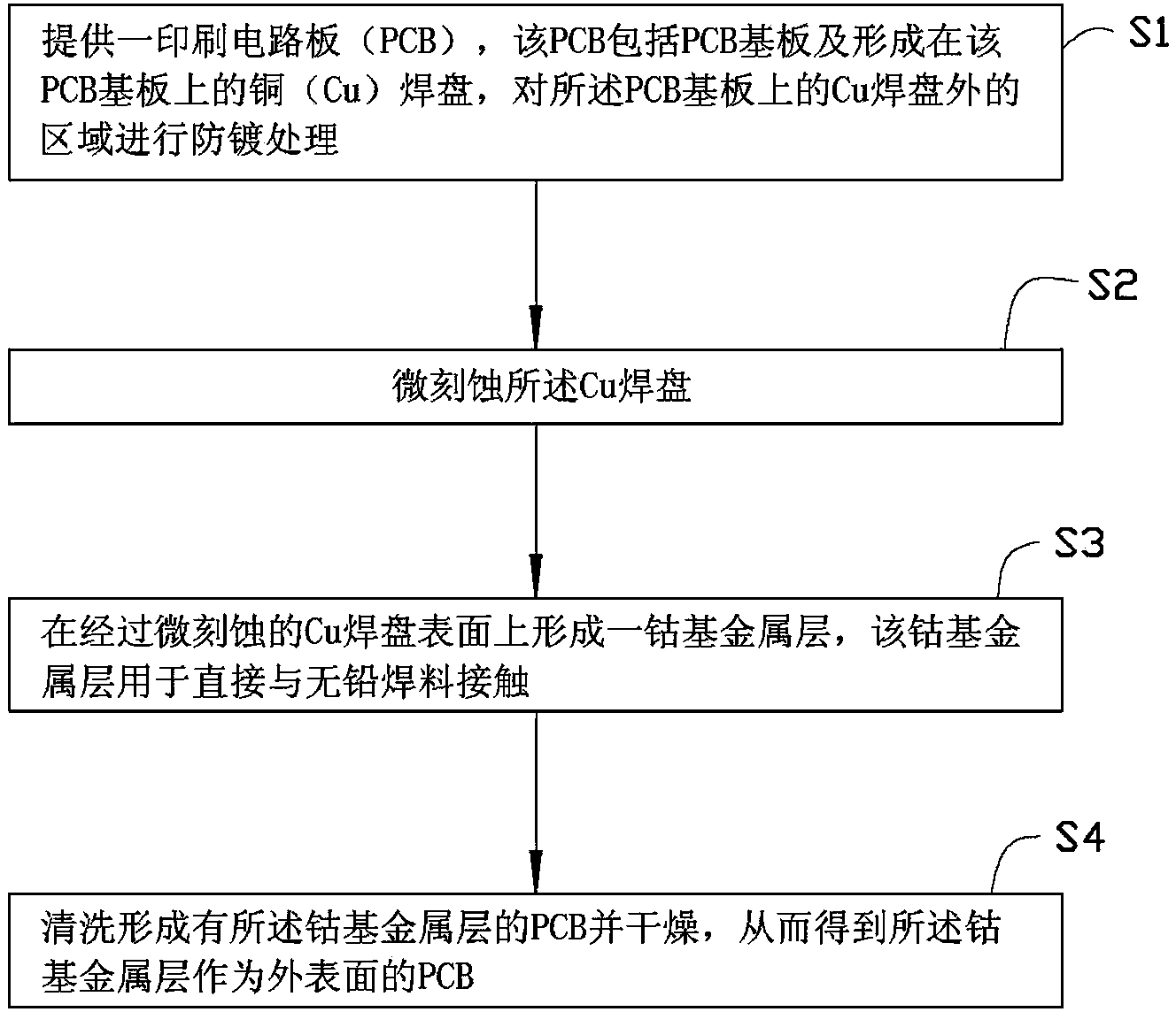
Printed circuit board and method for processing surface of printed circuit board
A printed circuit board and surface treatment technology, applied in the directions of printed circuit, printed circuit manufacturing, electrical components, etc., can solve the problems of difficult control, affecting the reliability of lead-free solder solder joints, solder joint failure, etc., to reduce process links, The appearance is white and bright, not easy to fatigue and creep effect
- Summary
- Abstract
- Description
- Claims
- Application Information
AI Technical Summary
Problems solved by technology
Method used
Image

Examples
Embodiment 1
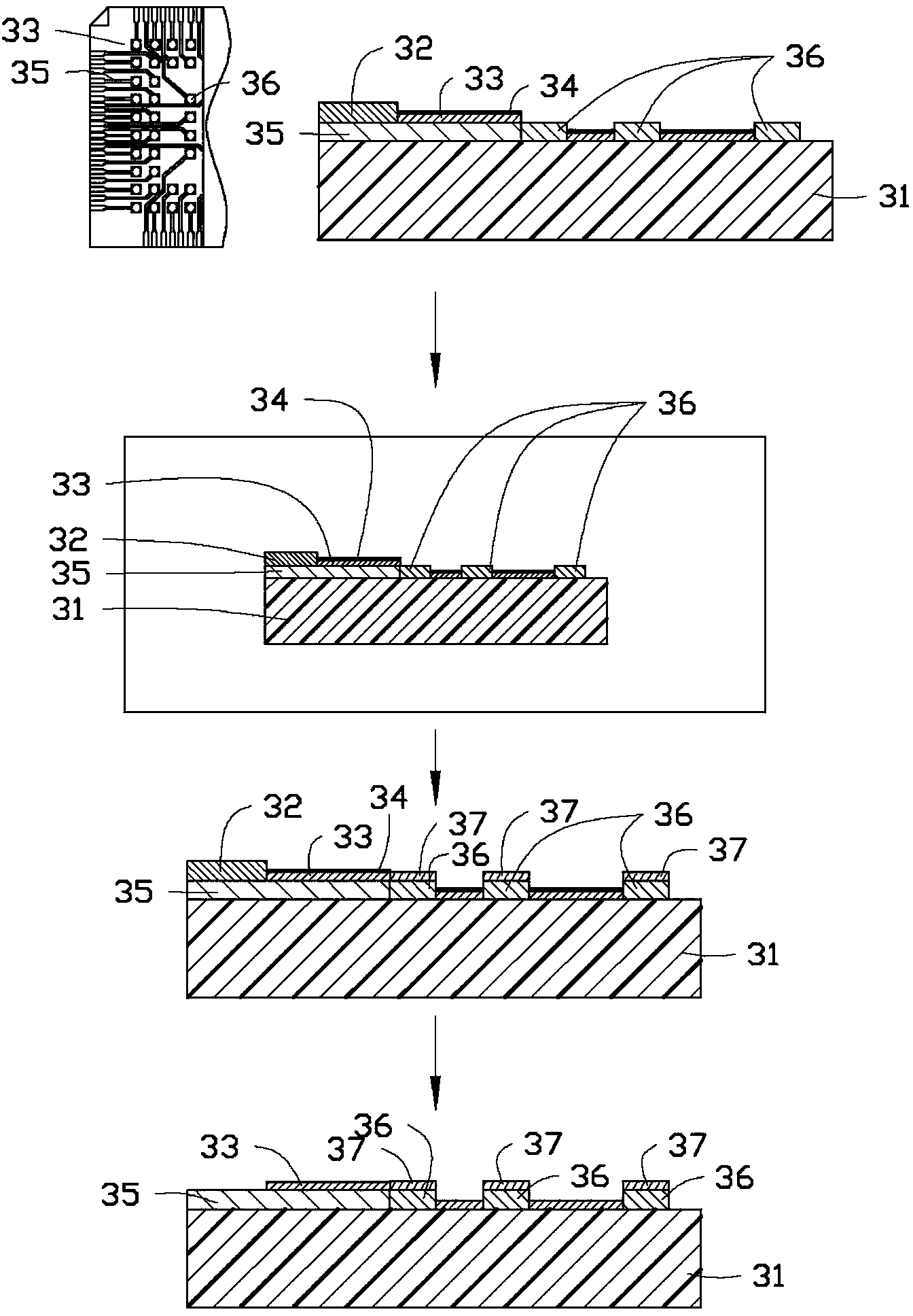
[0042] see figure 2 , a PCB surface treatment method for semiconductor packaging comprising the steps of:
[0043] (1) Apply solder resist on the area other than the circular Cu pad 36 on the PCB substrate 31 that needs surface treatment, including the output wire 35, and dry it to form a solder resist area 33, and evenly coat the surface of the solder resist area 33 with Cover a layer of anti-plating film 34, and cover the peripheral area that does not need electroplating with adhesive tape 32 after the input / output ends of the wires are connected; use ultrasonic cleaning to form the PCB substrate 31 with the above-mentioned anti-plating agent / adhesive tape and dry, wherein, the Cu welding The disc 36 has a diameter of 0.5 mm;
[0044] (2) Put the cleaned PCB into the plasma cleaning equipment for micro-etching for 3 minutes. The working gas is a mixed gas of argon and air. The flow rate of the working gas is 10SCCM and the power is 0.2KW. 0.9 Pa;
[0045] (3) The cobalt-...
Embodiment 2
[0051] see figure 2 , a PCB surface treatment method for semiconductor packaging comprising the steps of:
[0052] (1) Same as embodiment 1;
[0053] (2) Same as Example 1, wherein the micro-etching treatment time is 4 minutes, the flow rate of the working gas is 9SCCM, the power is 0.3KW, and the pressure in the cavity is kept at 0.8 Pa by a vacuum pump;
[0054] (3) Electroplating is used to form a cobalt-based metal layer 37 on the surface of the PCB. The anode used for electroplating is a cobalt sheet, the cathode is a circular Cu pad on the PCB, and the electroplating solution is composed of CoCl with a concentration of 0.15mol / L. 2·6H 2 O, CoCO at a concentration of 0.095mol / L 3 , the concentration is 0.35mol / L of H 3 PO 4 , the concentration is 0.15mol / L of H 3 PO 3 , the concentration is 0.02 g / L sodium saccharin, the temperature is 75°C, and the current density is 3.5A / dm 2 , the coating time is 8min, and ultrasonic assisted deposition is applied;
[0055] (...
Embodiment 3
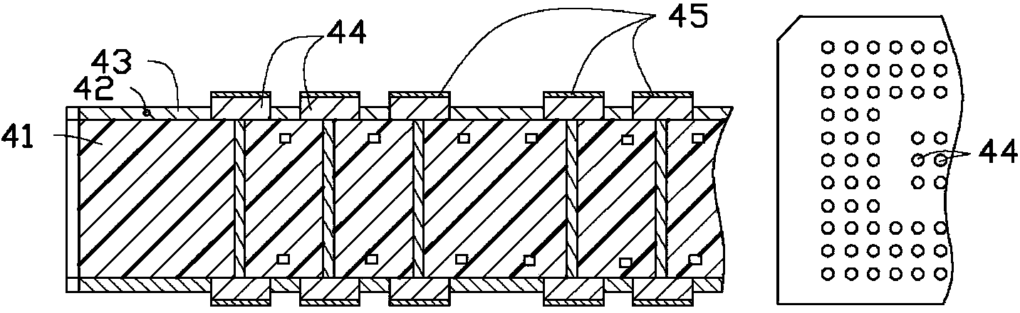
[0060] A method for surface treatment of an IC mounting surface substrate for packaging is obtained as image 3 Shown is a packaged IC mounting surface substrate formed with a cobalt-based metal layer. The surface treatment method comprises the following steps:
[0061] (1) Apply solder resist on the area of the IC mounting surface substrate 41 that requires surface treatment other than the surface mount Cu pad 44 and dry to form a solder resist area 42, and evenly coat a layer of anti-solder on the surface of the solder resist area 42. The coating 43 is finally cleaned and dried with ultrasonic water, wherein the diameter of the Cu pad 36 is 0.5 mm;
[0062] (2) Put the cleaned PCB into the plasma cleaning equipment for micro-etching for 8 minutes. The working gas is a mixed gas of argon and air, the flow rate is 5SCCM, the power is 0.4KW, and the pressure in the cavity is kept at 1 Pa by a vacuum pump;
[0063] (3) After activating the IC mounting surface substrate with ...
PUM
 Abstract
Description
Claims
Application Information