Zinc oxide pressure-sensitive resistor and preparation method thereof
A piezoresistor and zinc oxide technology, which is applied in the direction of piezoresistor core, piezoresistor, and resistors with lead-outs, can solve the problem of uneven distribution of current density, easy burning of electrode layers, and easy detachment of electrode layers and other problems, to achieve the effect of good process consistency and repeatability, green and environmental protection in the preparation process, and low production cost
- Summary
- Abstract
- Description
- Claims
- Application Information
AI Technical Summary
Problems solved by technology
Method used
Image
Examples
Embodiment 1
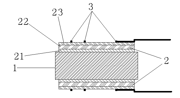
[0044] This example is a production process for preparing a three-layer film electrode layer by sputtering on the surface of a zinc oxide varistor ceramic substrate with a diameter of Ф10mm and a thickness of 2mm and a model of 10471K. The bottom transition layer is chromium, and the intermediate barrier layer is nickel copper. Alloy, the surface welding layer is silver.
[0045] Put the high-temperature sintered zinc oxide varistor ceramic substrate into a ball mill for rolling washing for 30 minutes, then ultrasonically clean it in tap water and deionized water for 20 minutes, and dry it in an oven at 120°C for 20 minutes; Put the cleaned and dried ceramic substrate into the special mask fixture, and then install the mask fixture on the workpiece holder; send the workpiece holder into the multi-target sputtering coating equipment, and vacuum the equipment cavity, Make the vacuum in the cavity reach 5×10 -3 Pa; fill the vacuum chamber with high-purity argon, and dynamically ...
Embodiment 2
[0048] This example is the production process of sputtering on the surface of a 14561K zinc oxide varistor ceramic substrate with a diameter of Ф14mm and a thickness of 2mm to prepare two layers of film electrode layers. The bottom transition layer is chromium and the surface welding layer is copper.
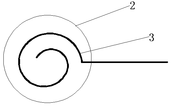
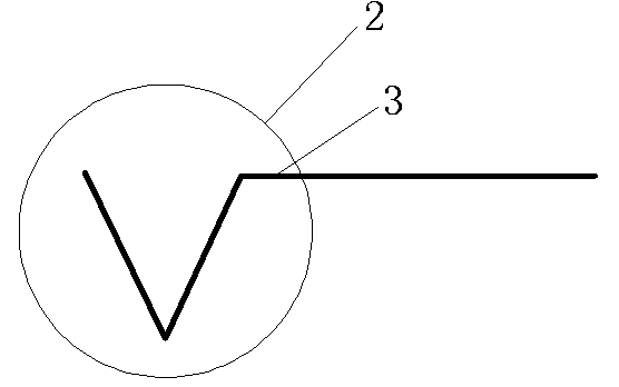
[0049] In this embodiment, except that there is no intermediate barrier layer and copper is used as the surface soldering layer, other process steps are the same as those in Embodiment 1, and will not be repeated here. The bottom transition layer in the two-layer film system electrode layer is made of chromium film with a thickness of 200nm, and the surface welding layer is made of copper with a thickness of 2800nm. After the sputtering is completed, an anti-oxidation process is carried out on the surface of the surface welding layer, and coil-like electrode leads are welded on the surface welding layer, and the performance is measured after packaging.
[0050] For zinc oxide va...
PUM
| Property | Measurement | Unit |
|---|---|---|
| thickness | aaaaa | aaaaa |
| thickness | aaaaa | aaaaa |
| thickness | aaaaa | aaaaa |
Abstract
Description
Claims
Application Information


