

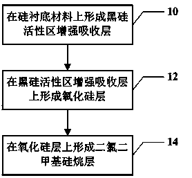
Black silicon super-hydrophobic material and manufacturing method thereof
A superhydrophobic and black silicon technology, applied in the field of nanomaterials, can solve the problems of high reflectivity infrared non-response restriction development, etc., to achieve the effect of ensuring high-quality operation, simple operation, and simple preparation process
- Summary
- Abstract
- Description
- Claims
- Application Information
AI Technical Summary
Problems solved by technology
Method used
Image

Examples
example 1
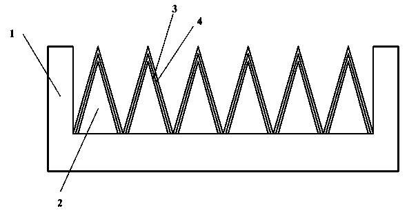
[0052] An N-type (100) single crystal silicon chip with a resistivity of 2-8 ohms (Ohm) is ultrasonically cleaned in trichlorethylene, acetone, and methanol solutions in sequence. After rinsing with deionized water and blowing dry with nitrogen, thermally evaporate the tellurium film in vacuum with an evaporation rate of 2-3nm / s and a thickness of 500nm. Put the coated silicon wafer on the three-dimensional movable target stage in the vacuum chamber, the pressure in the chamber is lower than 10-2mbar, the working gas is air, and the working pressure is 500Torr. The silicon wafer is irradiated with a titanium sapphire femtosecond laser, the wavelength of the light source is 800nm, the pulse width is 180fs, and the pulse frequency is 1kHz. Pulse energy range 0.17-1.69J / cm 2 , at 4×4mm 2 Scan uniformly within the area, and control the number of pulses in the range of 300-3000. After testing, the absorption of black silicon is higher than 85% in the range of 250-400 nm, and hig...
example 2
[0054] Set the size to 23×23mm 2 The N-type (100) single crystal silicon wafer with a resistivity of 2-8 Ohm was cleaned by the standard RCA method (that is, the standard wet chemical cleaning method), and ultrasonic was used for 15 minutes per step. The beakers, graduated cylinders, hydrofluoric acid-resistant tweezers, rubber-tip droppers, etc. used to prepare the solution were ultrasonically cleaned with acetone, ethanol, and deionized water for 15 minutes each. The chemical corrosion solution is configured in a certain proportion, which is composed of hydrogen peroxide, ethanol, deionized water, hydrofluoric acid and chloroauric acid. Before the reaction, place the silicon wafer in 10% hydrofluoric acid solution to remove the natural oxide layer on the surface. During the reaction, the device was placed in a heat-collecting constant temperature magnetic stirrer, the temperature was set at 35° C., and a 2.5 cm magnetic rotor was selected. After testing, the black silicon ...
PUM
| Property | Measurement | Unit |
|---|---|---|
| temperature | aaaaa | aaaaa |
| thickness | aaaaa | aaaaa |
Abstract
Description
Claims
Application Information