Laser chemical order controllable preparation method of monocrystalline silicon inverted pyramid suede

An inverted pyramid and monocrystalline silicon technology, which is applied in semiconductor/solid-state device manufacturing, electrical components, circuits, etc., can solve the problems of complicated process steps and high equipment investment, and achieve the effects of simplified manufacturing process, low cost and simple operation

Inactive Publication Date: 2013-12-04
BEIJING UNIV OF TECH
View PDF10 Cites 12 Cited by
  • Summary
  • Abstract
  • Description
  • Claims
  • Application Information

AI Technical Summary

Problems solved by technology

(T.Juvonen, J.H and P.Kuivalainen, "HighEfficiencySingleCrystallineSiliconSolarCells", PhysicaScripta, T101, 96-98, 2002) It can be seen that, The preparation, opening and removal of etching masks are complicated process steps, which restrict production efficiency, and the corresponding equipment investment is relatively high

Method used


Image

  • Laser chemical order controllable preparation method of monocrystalline silicon inverted pyramid suede
  • Laser chemical order controllable preparation method of monocrystalline silicon inverted pyramid suede
  • Laser chemical order controllable preparation method of monocrystalline silicon inverted pyramid suede

Examples


Embodiment 1

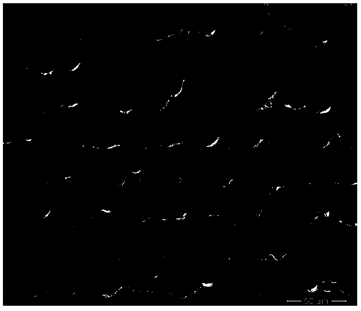
[0024] (1) Laser scanning opening positioning: use the focused 1064nm picosecond laser to scan the surface of the silicon wafer line by line, the diameter of the focused spot is 40 μm, the length of the scanning line is 8 mm, the scanning distance is 30 μm, and the energy density is 7.5 J / cm 2 , A=2.00*10 7 (Define A as the average number of pulses received per square centimeter on the surface of the silicon wafer), form evenly distributed inverted cone-shaped holes on the surface of the silicon wafer, with a diameter of about 30 μm, and finally obtain a square suede surface with a size of 8mm*8mm. Such as figure 1 ;

[0025] (2) pickling porous fleece layer: first rinse with HF acid with a volume fraction of 15% for 5 minutes to remove the generated oxides, then perform ultrasonic cleaning with distilled water for 5 minutes to remove debris, and then blow dry with nitrogen;

[0026] (3) Preparation of inverted pyramid suede: Put the pickled sample into the prepared alkaline...

Embodiment 2

[0032] (1) Preparation of hole-shaped suede surface: scan the surface of the silicon wafer line by line with a focused 1064nm picosecond laser, the diameter of the focused spot is 40 μm, the length of the scanning line is 8 mm, the scanning distance is 20 μm, and the energy density is 8.4 J / cm 2 , A=1.56*10 7 (Define A as the average number of pulses received per square centimeter on the surface of the silicon wafer), form evenly distributed inverted cone-shaped holes on the surface of the silicon wafer, with a diameter of about 20 μm, and finally obtain a square suede surface with a size of 8mm*8mm;

[0033] (2) pickling porous fleece layer: first rinse with HF acid with a volume fraction of 25% for 3 minutes to remove the generated oxides, then perform ultrasonic cleaning with distilled water for 3 minutes to remove debris, and then blow dry with nitrogen;

[0034] (3) Preparation of inverted pyramid suede: Put the pickled sample into the prepared alkaline solution and heat ...

Embodiment 3

[0040] (1) Preparation of hole-shaped suede: scan the surface of the silicon wafer line by line with a focused 1064nm picosecond laser, the diameter of the focused spot is 40 μm, the length of the scanning line is 8 mm, the scanning distance is 30 μm, and the energy density is 6.8 J / cm 2 , A=2.68*10 7 (Define A as the average number of pulses received per square centimeter on the surface of the silicon wafer), form evenly distributed inverted cone-shaped holes on the surface of the silicon wafer, with a diameter of about 30 μm, and finally obtain a square suede surface with a size of 8mm*8mm;

[0041] (2) pickling porous fleece layer: first rinse with HF acid with a volume fraction of 20% for 5 minutes to remove the generated oxides, then perform ultrasonic cleaning with distilled water for 5 minutes to remove debris, and then blow dry with nitrogen;

[0042] (3) Preparation of inverted pyramid suede: Put the pickled sample into the prepared alkaline solution and heat it in a ...


PUM

PropertyMeasurementUnit
diameteraaaaaaaaaa

Abstract

The invention discloses a laser chemical order controllable preparation method of a monocrystalline silicon inverted pyramid suede. The laser chemical order controllable preparation method comprises the following steps of 1 performing laser scanning, tapping and positioning, namely utilizing software to draw a required felting graph (computer aided design (CAD) drawing), performing the scanning and the tapping on the surface of a cleaned silicon wafer through picoseconds laser according to the graph to form a micron-sized inverted-cone-shaped suede with evenly-distributed holes; 2 performing acid washing of the poroid suede, firstly using hydrogen fluoride (HF) to perform the acid washing and then using distilled water to perform the washing; 3 performing acid washing of a poroid suede layer, firstly using the HF to perform acid washing and then using ultrapure water to perform washing; 4 preparing the inverted pyramid suede, namely placing a sample subjected to the acid washing into a prepared alkaline solution to perform heating in water bath so as to prepare the micron-sized inverted pyramid suede. A preparing and mask-removing process is omitted and replaced by a laser scanning and tapping technology, and the size and the shape of a felting region can be customized through the software (CAD). The monocrystalline silicon inverted pyramid suede has excellent reflection-reducing effect on a 400-700nm wave band with intensive solar spectrum photons, and the reflection rate reaches up to 5%.

Description

technical field [0001] The invention relates to the technical field of crystalline silicon solar cells, in particular to a laser chemical sequence controllable preparation method of a single crystal silicon inverted pyramid texture. Background technique [0002] In the photovoltaic industry, monocrystalline silicon and polycrystalline silicon solar cells have a dominant position and occupy most of the market share. Compared with polycrystalline silicon, monocrystalline silicon can more effectively prepare fleece layers with regular microstructure and low reflectivity, and solar cells based on monocrystalline silicon have higher photoelectric conversion efficiency. Texture on the surface of monocrystalline silicon usually adopts a wet etching process, that is, the surface of the silicon wafer (100) is treated with an alkaline solution (such as sodium hydroxide solution, etc.). Due to anisotropic corrosion, the surface will be uneven, thus Increase the optical path to achieve...

Claims


Application Information

Patent Timeline
Patent Type & Authority Applications(China)
IPC IPC(8): H01L21/268H01L21/306
Inventor 季凌飞吕晓占吴燕凌晨胡炎蒋毅坚王世贤
Owner BEIJING UNIV OF TECH
Why Eureka
Try Eureka