Memory unit of low-power resistive random access memory and preparation method of memory unit

A resistive random and storage unit technology, applied in static memory, digital memory information, electrical components, etc., can solve the problems of complex metal oxide formation process, pollution, and difficult control of film composition ratio, so as to reduce reset Operating current and reading current, increasing the resistance value, and reducing the effect of reading and writing power consumption

Active Publication Date: 2013-12-04
中国科学院上海硅酸盐研究所苏州研究院
View PDF5 Cites 4 Cited by
  • Summary
  • Abstract
  • Description
  • Claims
  • Application Information

AI Technical Summary

Problems solved by technology

But in the process of making the actual resistive memory, image 3 The current control layer in the structure shown is formed by methods such as CVD or sputtering. The formation process of oxides of transition metal elements and multi-component doped metal oxides is quite complicated, especially metal-doped oxides, which are used in conventional integrated circuits. It is difficult to control the composition ratio of the thin film in the production method, and the transition metal elements have certain pollution to the CMOS integrated circuit process equipment

Method used


Image

  • Memory unit of low-power resistive random access memory and preparation method of memory unit
  • Memory unit of low-power resistive random access memory and preparation method of memory unit
  • Memory unit of low-power resistive random access memory and preparation method of memory unit

Examples


Embodiment 1

[0063] (1) On a clean silicon substrate, grow a layer of silicon oxide by thermal oxidation, and then use acetone to sonicate, and then heat and clean it in a cleaning solution of ammonia water plus hydrogen peroxide, hydrochloric acid and hydrogen peroxide. The thermal oxidation temperature is 900-1100°C, and the SiO produced by thermal oxidation 2 The layer thickness is 400-600 nm.

[0064] (2) Deposit the bottom electrode on the cleaned surface. The material of the bottom electrode film can be any one of Pt, Au, Ni, Ti, W, Mo, Al, Ag-Al alloy, ITO or FTO. The thickness of the bottom electrode film is 50-100nm.

[0065] (3) Weigh the analytically pure V 2 o 5 Powder, high purity and good stability V 2 o 5 Sol.

[0066] (4) Molar ratio (aniline: V 2 o 5 ) is 0.25:1, weigh 1ml aniline, add 10ml water to make a solution, add monomer dropwise and add 50mlV 2 o 5 In the sol, stir fully on a magnetic stirrer at room temperature, react for 24 hours, and finally form dark ...

Embodiment 2

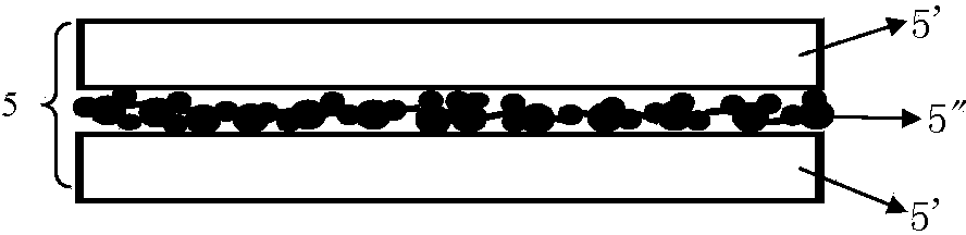
[0074]Replace the aniline in step (4) in Example 1 with dodecylamine for intercalation reaction, and then photolithography and etching in the upper end region of the tubular electrode to form a multilayer film unit composed of a storage film and an intercalation composite film block as a storage medium. Others are similar to Embodiment 1, and similar effects can also be achieved.


PUM


Abstract

The invention relates to a memory unit of a low-power resistive random access memory and a preparation method of the memory unit. The memory unit comprises a top electrode, a memory material/organic molecular compound layer, a bottom electrode and a substrate, the memory material/organic molecular compound layer is a compound layer formed by intercalating organic molecules between layered resistive memory materials through a molecule intercalation technology, the layered resistive memory materials are layered oxides or chalcogenides, and the organic molecules are alkylamine, polyaniline, polypyrrole or polythiophene.

Description

technical field [0001] The invention relates to a multi-layer film unit of a low power consumption resistive RAM based on molecular intercalation technology and a preparation method thereof. Background technique [0002] With the rapid development of information technology, the research and development of high-speed, large-capacity permanent storage has become a necessary condition to promote the rapid development of digital technology. Resistive random access memory (RRAM) refers to a new type of memory that uses the high and low resistance states of memory cells to store data under the action of an external electric field. The basic structure of the RRAM device is composed of metal electrode / oxide film / metal electrode (MOM). During the RRAM storage process, a programmable voltage is used to drive the migration of oxygen vacancies in the ultra-high-density crossbar array in the RRAM device. Change the resistance value of the bit cell. With its advantages of simple structu...

Claims


Application Information

Patent Timeline
Patent Type & Authority Applications(China)
IPC IPC(8): H01L45/00G11C13/00B82Y10/00
Inventor 王群陈立东
Owner 中国科学院上海硅酸盐研究所苏州研究院
Why Eureka
Try Eureka