Fluorine-doped diamond-like film, preparation method thereof and impressing template comprising fluorine-doped diamond-like film
A diamond film and fluorine technology, applied in the field of nano-processing, can solve the problems of low surface free energy, lack of hydrophobic properties, unsuitable for nano-imprint template anti-stick coating, etc., to reduce surface energy, improve hydrophobic performance and Anti-adhesion performance, the effect of improving the reuse rate
- Summary
- Abstract
- Description
- Claims
- Application Information
AI Technical Summary
Problems solved by technology
Method used
Image

Examples
Embodiment 1
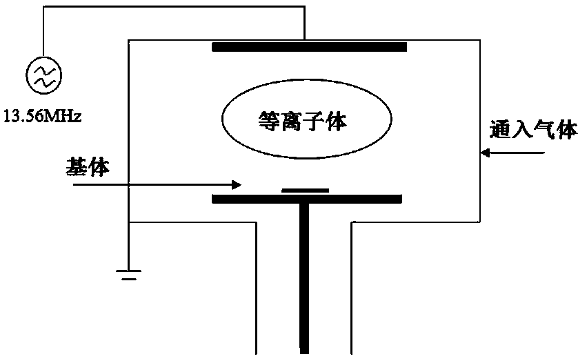
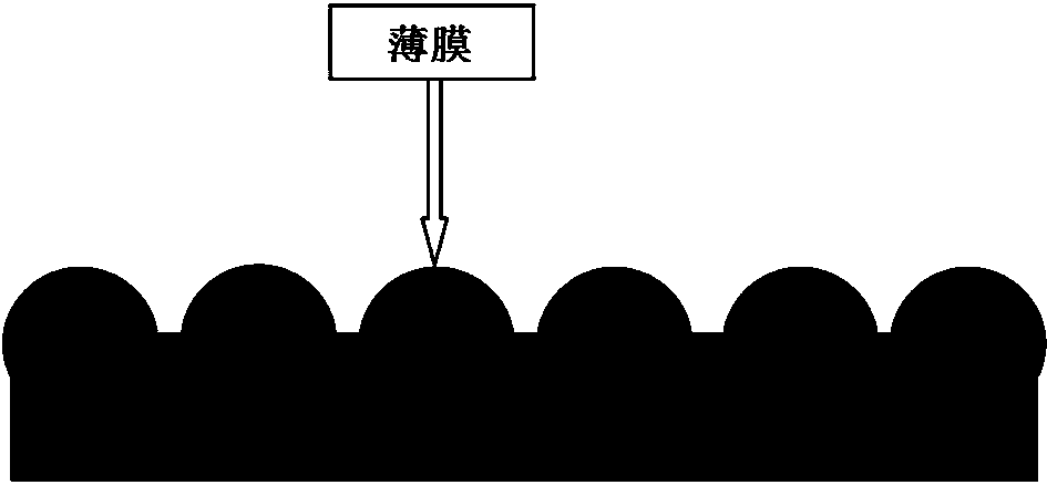
[0028] By plasma-enhanced chemical vapor deposition, the figure 1 It is a schematic diagram of the plasma-enhanced chemical vapor deposition device involved. Specifically, the soft template (polydimethylsiloxane) for nanoimprinting is placed in the chamber of the plasma device, and the vacuum is evacuated to 1.0×10 -3 Pa; then pass Ar gas to a vacuum of 2.0Pa, turn on the radio frequency power supply, the power of the radio frequency power supply is 100W, perform glow discharge, and use argon plasma to activate and clean the surface of the soft template; then pass CF 4 、CH 4 Mixed gas with Ar, CH 4 、CF 4 The mass flow percentages of Ar and Ar are 74%, 7%, and 19% respectively, so that the total pressure is 4.0Pa. Turn on the RF power supply. The power of the RF power supply is 200W. The mixed gas glow discharges to generate plasma. The discharge time is the deposition time. In 1 minute, the fluorine-doped diamond-like anti-adhesive film is deposited and formed on the imprin...
Embodiment 2
[0030] Using the plasma-enhanced chemical vapor deposition method, the hard template (silicon wafer) for nanoimprinting was placed in the chamber of the plasma device, and the vacuum was evacuated to 1.0×10 -3 Pa; then pass Ar gas to a vacuum of 2.0Pa, turn on the RF power supply, the power of the RF power supply is 100W, perform glow discharge, and use argon plasma to activate and clean the surface of the hard template; then pass CF 4 、CH 4 Mixed gas with Ar, CH 4 、CF 4 The mass flow percentages of Ar and Ar are 67%, 10%, and 23% respectively, so that the total pressure is 4.0Pa. Turn on the RF power supply. The power of the RF power supply is 200W. The mixed gas glow discharges to generate plasma. The discharge time is the deposition time. In 3 minutes, the DLC anti-adhesive film is deposited on the imprint template, the thickness of the anti-adhesive film is 10 nm, the fluorine content is 3%, and the deposition temperature is 200 degrees.
Embodiment 3
[0032] Using the magnetron sputtering method, place the hard template (quartz) for nanoimprinting in the vacuum sputtering chamber, use graphite with a purity of 99.99% as the target, and the operating frequency of the RF power supply is 13.56MHz, between the target cathode and the substrate stage The distance is about 40mm; vacuumize to 2.0×10 -3 Pa, enter Ar gas until the vacuum degree is 2.0Pa, turn on the RF power supply, the power of the RF power supply is 100W, perform pre-sputtering, and clean the target surface with argon plasma; then pass CHF 3 Gas until the working pressure is 4.0Pa, turn on the radio frequency power supply, the radio frequency power supply power is 150W, sputter the target material, the sputtering time is 5 minutes, promptly deposit the described DLC anti-adhesive film on the embossing template, the described anti-adhesive film The film thickness is 8nm, the fluorine content is 2%, and the deposition temperature is 25 degrees.
PUM
| Property | Measurement | Unit |
|---|---|---|
| thickness | aaaaa | aaaaa |
| thickness | aaaaa | aaaaa |
| thickness | aaaaa | aaaaa |
Abstract
Description
Claims
Application Information
 - R&D
- Intellectual Property
- Life Sciences
- Materials
- Tech Scout
- Unparalleled Data Quality
- Higher Quality Content
- 60% Fewer Hallucinations
Browse by: Latest US Patents, China's latest patents, Technical Efficacy Thesaurus, Application Domain, Technology Topic, Popular Technical Reports.
© 2025 PatSnap. All rights reserved.Legal|Privacy policy|Modern Slavery Act Transparency Statement|Sitemap|About US| Contact US: help@patsnap.com