Back electrode of solar battery device, preparation method of back electrode and solar battery device

A solar cell and back electrode technology, applied in electrical components, semiconductor devices, circuits, etc., can solve problems such as mismatch, lower photoelectric conversion efficiency, and high interface material lattice, so as to reduce the density of interface defect states and improve photoelectric conversion Efficiency, the effect of reducing the surface recombination rate

Active Publication Date: 2013-12-25
SHENZHEN INST OF ADVANCED TECH +1
View PDF3 Cites 12 Cited by
  • Summary
  • Abstract
  • Description
  • Claims
  • Application Information

AI Technical Summary

Problems solved by technology

[0003] However, there is a high density of defect states at the interface between the metal back electrode and the light-absorbing layer of the p-type semiconductor film, which is caused by the unsaturated dangling bonds of the interface atoms and the lattice mismatch of the interface material. recombination pathway
As the minority carriers in p-type semiconductors, electrons are easily captured by defect levels when they appear near this interface, and then transition to the valence band and recombine with holes through the defect level, which reduces the carrier collection efficiency, thereby reducing the solar energy. The photoelectric conversion efficiency of the battery device affects the performance of the thin film solar cell device
According to reports, in copper indium gallium selenide (CIGS) thin film solar cells, the interfacial recombination rate (SRV) of CIGS thin film light absorbing layer and metal Mo back electrode is as high as 10 3 ~10 6 cm / s, which seriously reduces the photoelectric conversion efficiency of solar cell devices
[0004] Moreover, as the thickness of the light-absorbing layer decreases, the metal Mo back electrode interface is closer to the light-absorbing region in the light-absorbing layer, and more photogenerated carrier pairs are generated near the interface, thereby recombining through defect levels. , therefore, the conventional form of the metal back electrode restricts the thickness of the light-absorbing layer of thin-film solar cell devices to develop in a thinner direction

Method used


Image

  • Back electrode of solar battery device, preparation method of back electrode and solar battery device
  • Back electrode of solar battery device, preparation method of back electrode and solar battery device
  • Back electrode of solar battery device, preparation method of back electrode and solar battery device

Examples


preparation example Construction

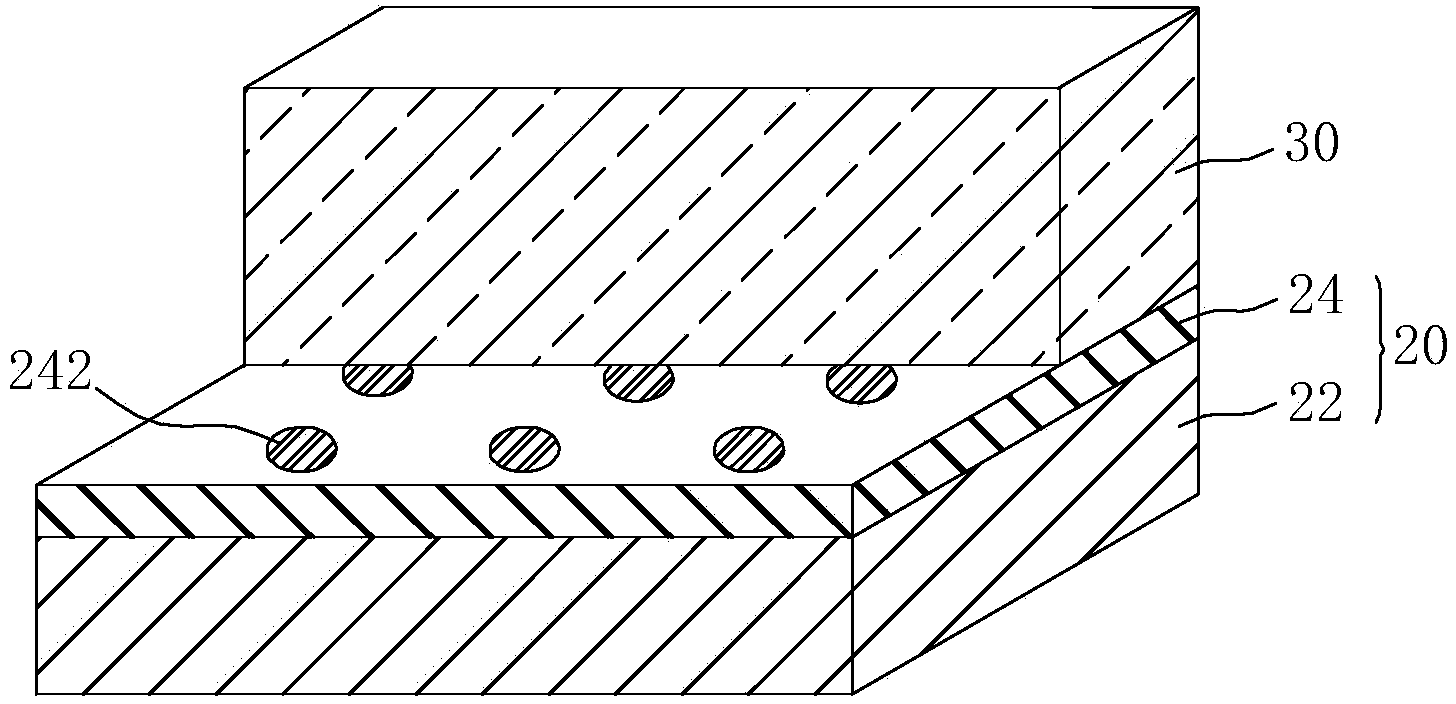
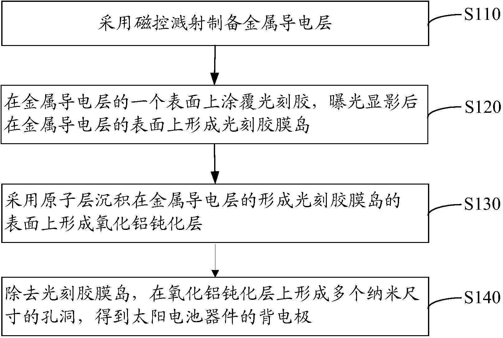
[0051] see image 3 , the preparation method of the back electrode of the solar cell device of an embodiment, comprises the following steps:

[0052] Step S110: Preparing a metal conductive layer by magnetron sputtering.

[0053] A substrate is provided, which can be a soda-lime glass substrate or other flexible material substrate (stainless steel foil, titanium foil or polyimide substrate, etc.).

[0054] After cleaning and drying the substrate, put it on the sample holder of the magnetron sputtering vacuum chamber, the vacuum degree of the magnetron sputtering vacuum chamber is 2×10 -4 After Pa, turn on the heating power of the sample holder, and maintain the sample holder at 250°C. Introduce argon or a mixed gas of argon and oxygen, adjust the flow meter to control the inflow rate of the gas to 12.5 sccm, and adjust the air pressure in the magnetron sputtering vacuum chamber to 0.1-1 Pa, preferably 0.16 Pa.

[0055] Adjust the sputtering power of molybdenum target or alu...

Embodiment 1

[0113] Fabrication of solar cell devices

[0114] (1) Provide a soda-lime glass substrate, clean and dry the soda-lime glass substrate and put it on the sample holder of the magnetron sputtering vacuum chamber, heat the temperature of the sample holder to 250°C, and the vacuum degree is 0.16Pa , with a power density of 4W / cm 2 Sputtering metal molybdenum onto the soda-lime glass substrate to form a metal conductive layer laminated on the soda-lime glass substrate with a thickness of 1 micron;

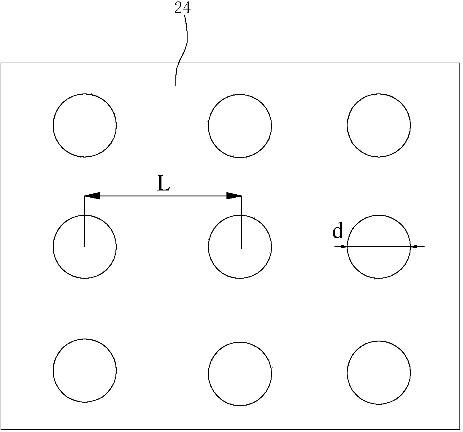
[0115] (2) Spin coat photoresist NR5-8000 on the metal conductive layer, spin coating speed 1000rpm, spin coating time 40 seconds, and then bake at 150°C for 10 minutes to cure the photoresist to form a layer on the metal conductive layer on a 15 µm thick photoresist layer. Expose and develop the photoresist layer with the designed mask. There are multiple circular holes on the mask plate, the diameter of each circular hole is 1 micron, the distance between the centers of the cross-s...

Embodiment 2

[0120] Fabrication of solar cell devices

[0121] (1) Provide a soda-lime glass substrate, clean and dry the soda-lime glass substrate and put it on the sample holder of the magnetron sputtering vacuum chamber, heat the temperature of the sample holder to 250°C, and the vacuum degree is 0.16Pa , with a power density of 4W / cm 2 Sputtering metal molybdenum onto the soda-lime glass substrate to form a metal conductive layer laminated on the soda-lime glass substrate with a thickness of 2 microns;

[0122] (2) Spin coat photoresist NR5-8000 on the metal conductive layer, spin coating speed 1000rpm, spin coating time 40 seconds, and then bake at 150°C for 10 minutes to cure the photoresist to form a layer on the metal conductive layer on a 15 µm thick photoresist layer. Expose and develop the photoresist layer with the designed mask. There are multiple circular holes on the mask plate, the diameter of each circular hole is 1.5 microns, the distance between the centers of the cro...


PUM


Abstract

The invention relates to a back electrode of a solar battery device, a preparation method of the back electrode and the solar battery device. The back electrode of the solar battery device comprises a metal conducting layer and an aluminum oxide passivation layer stacked on the metal conducting layer. A plurality of nanoscale holes are formed in the aluminum oxide passivation layer. The metal conducting layer serves as the positive electrode of the solar battery device and is used for collecting and transmitting the current. The surface carrier recombination is restrained through the aluminum oxide passivation layer, current channels are formed by the multiple nanoscale holes to be used for collecting and breaking over the current, the back electrode of the composite structure gives the passivation effect of the aluminum oxide passivation layer and does not obstruct passing of the photo-generated current, and the effects of reducing the interface defect mode density, reducing the surface recombination rate of photo-generated carriers and improving the photoelectric converting efficiency of the solar battery device are achieved.

Description

technical field [0001] The invention relates to the technical field of photovoltaic devices, in particular to a back electrode for a solar cell device, a preparation method thereof, and a solar cell device. Background technique [0002] At present, the back electrode in conventional thin film solar cell devices is generally a metal thin film conductive layer, such as metal molybdenum (Mo) conductive layer. On the back electrode, the metal back electrode is in contact with the light-absorbing layer of the p-type semiconductor film, which serves as the "+" pole of the battery. [0003] However, there is a high density of defect states at the interface between the metal back electrode and the light-absorbing layer of the p-type semiconductor film, which is caused by the unsaturated dangling bonds of the interface atoms and the lattice mismatch of the interface material. Composite pathways occur. As the minority carriers in p-type semiconductors, electrons are easily captured ...

Claims


Application Information

Patent Timeline
Patent Type & Authority Applications(China)
IPC IPC(8): H01L31/0224H01L31/18
CPCY02P70/50
Inventor 宋秋明李朝晖谭兴顾光一陈旺寿肖旭东
Owner SHENZHEN INST OF ADVANCED TECH
Why Eureka
Try Eureka