Light trapping structure on silicon substrate surface, preparation method and application thereof

A light trapping structure, silicon substrate technology, applied in photovoltaic power generation, final product manufacturing, sustainable manufacturing/processing, etc., to achieve the effect of reducing reflection, increasing absorption and utilization

Inactive Publication Date: 2014-01-01
NANKAI UNIV
View PDF5 Cites 12 Cited by
  • Summary
  • Abstract
  • Description
  • Claims
  • Application Information

AI Technical Summary

Problems solved by technology

However, due to the limitations of the material properties of the silicon substrate itself and the corresponding chemical wet etching process, the size of the prepared pyramid is usually about 10 μm, and the average integral reflection of the total silicon wafer after texturing is usually about 10%, with nearly 10% of the light is reflected and not absorbed by the solar cell

Method used


Image

  • Light trapping structure on silicon substrate surface, preparation method and application thereof
  • Light trapping structure on silicon substrate surface, preparation method and application thereof
  • Light trapping structure on silicon substrate surface, preparation method and application thereof

Examples


Embodiment 1

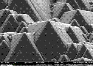
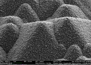
[0027] A method for preparing a light-trapping structure on the surface of a silicon substrate, first using NaOH, IPA and NaSiO 3 Carry out texturing, then use hydrofluoric acid and other reagents for smoothing, and finally use MOCVD technology to deposit nano-sized pyramids on the texturing silicon wafer to obtain a light-trapping structure that improves the surface of the silicon substrate. The steps are as follows:

[0028] 1) Place the silicon wafer in ethanol / acetone and sonicate for 5 minutes each to remove organic matter;

[0029] 2) Place the cleaned silicon wafer in a sodium hydroxide solution, heat the solution to 80°C, and react for 20 minutes to remove the damaged layer;

[0030] 3) Place the above silicon wafer in 74g of NaOH with a mass percentage concentration of 1%, 444ml of isopropanol with a volume percentage concentration of 6%, and 74g of NaSiO with a mass percentage concentration of 1%. 3 Add 6000ml of deionized water to the mixed solution of deionized wa...

Embodiment 2

[0037] A method for preparing a light-trapping structure on the surface of a silicon substrate, steps 1)-5) are the same as in Example 1, except for step 6):

[0038] 6) Put the Smooth-treated silicon wafer in the deposition chamber of MOCVD, the deposition temperature is 170°C, the flow rate of water vapor is 110 sccm, and the flow rate of DEZn is 180 sccm, B 2 h 6 The flow rate is 3 sccm, the deposition gas pressure is 1 Torr, the deposition time is 5 min, and the thickness of the ZnO layer is 300 nm, so that the light-trapping structure that improves the surface of the silicon substrate can be prepared.

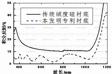
[0039] The technical effect of the light trapping structure is similar to that of Embodiment 1.

Embodiment 3

[0041] A method for preparing a light-trapping structure on the surface of a silicon substrate, steps 1)-5) are the same as in Example 1, except for step 6):

[0042] 6) Place the processed silicon wafer in the deposition chamber of MOCVD, the deposition temperature is 177°C, H 2 O steam flow is 130sccm, DEZn flow is 180sccm, B 2 h 6 The flow rate is 0 sccm, the deposition gas pressure is 0.8 Torr, the deposition time is 15 min, and the thickness of the ZnO layer is 900 nm, so that the light-trapping structure that improves the surface of the silicon substrate can be prepared.

[0043] The technical effect of the light trapping structure is similar to that of Embodiment 1.


PUM

PropertyMeasurementUnit
thicknessaaaaaaaaaa
electrical resistanceaaaaaaaaaa
reflectanceaaaaaaaaaa

Abstract

The invention relates to a light trapping structure on a silicon substrate surface, which is composed of a texturized monocrystalline silicon layer on the silicon substrate surface and a nano-size small pyramidal ZnO layer on texturized big pyramids, wherein the thickness of the ZnO layer is 300-1000nm, and the average light reflectivity of the light trapping structure for 400-1100nm wavelength is less than 10%. The preparation method comprises the following steps: texturizing on the silicon substrate surface by using sodium hydroxide, isopropanol and sodium silicate, carrying out smoothing treatment by using a mixed solution of hydrofluoric acid, nitric acid and acetic acid, and finally, depositing the nano-size pyramids on the texturized silicon chip by using an MOCVD (metal-organic chemical vapor deposition) technique. The light trapping structure can be used for a HIT cell using monocrystalline silicon as the substrate. The light trapping structure can lower the reflection of the texturized silicon substrate surface etched by a wet process, is used for a silicon geterojunction cell using monocrystalline silicon as the substrate, and can enhance the visible light absorption and utilization of the solar cell.

Description

technical field [0001] The invention belongs to the preparation technology of solar cells, in particular to a light-trapping structure on the surface of a silicon substrate and its preparation method and application. Background technique [0002] People have a long history of research on solar cells. In 1839, Becquerel discovered the photovoltaic effect. After more than 100 years of theoretical research and experiments, in 1954, Chapin and others at Bell Laboratories in the United States produced the first solar cell. Since then, research on solar cells made of other materials such as amorphous (microcrystalline) silicon thin-film solar cells, cadmium telluride solar cells (CdTe), copper indium gallium selenide solar cells (CIGS), etc. has also continued. However, At present, crystalline silicon solar cells are mainly used in photovoltaic power generation. Because of their high efficiency, stable performance, rich materials, and non-toxicity, they still occupy the mainstrea...

Claims


Application Information

Patent Timeline
Patent Type & Authority Applications(China)
IPC IPC(8): H01L31/0216H01L31/0224H01L31/052H01L31/18
CPCY02E10/52Y02E10/50H01L31/022483H01L31/02366H01L31/074H01L31/1884Y02P70/50
Inventor 张晓丹陈新亮魏长春赵颖
Owner NANKAI UNIV
Why Eureka
Try Eureka