Method for preparing self-sustained silicon nanowire array

A silicon nanowire array and metal mesh technology, applied in the field of nanomaterials, can solve the problem of not obtaining a two-dimensional silicon nanowire array, and achieve the effect of cheap raw materials, rapid preparation, and high purity

Active Publication Date: 2014-02-12
ZHANGJIAGANG IND TECH RES INST CO LTD DALIAN INST OF CHEM PHYSICS CHINESE ACADEMY OF SCI +1
View PDF5 Cites 3 Cited by
  • Summary
  • Abstract
  • Description
  • Claims
  • Application Information

AI Technical Summary

Problems solved by technology

CN 101736354A reported the use of molten salt electrochemical method by SiO 2 Materials such as silicon nanoparticles a

Method used


Image

  • Method for preparing self-sustained silicon nanowire array
  • Method for preparing self-sustained silicon nanowire array
  • Method for preparing self-sustained silicon nanowire array

Examples


Embodiment 1

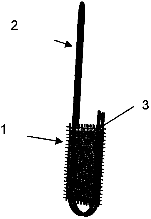
[0037] (a) JGS3 optical quartz plate with a size of 20x10x0.5mm. Two pieces of 20x10mm 20-mesh metal nickel mesh are used as current collectors, clamped and fixed with metal molybdenum wires with a diameter of 1mm to make working electrodes.

[0038] (b) CaCl at 850 °C in a molten salt electrochemical device under an argon atmosphere 2 In the molten salt, 1.9V voltage is used for electrodeoxidation, and the graphite crucible is used as the counter electrode, and the reaction time is about 5h.

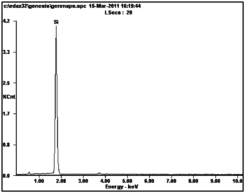
[0039] (c) After the reaction is completed, remove the working electrode from the salt solution, cool it under an inert atmosphere, take it out and wash it in water, and strip off the nickel mesh, molybdenum wire and outer impurities, and the obtained product is a silicon nanowire array.

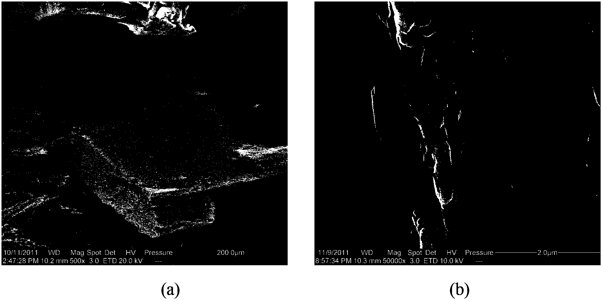
[0040] The silicon nanowire array has two layers, each layer has a thickness of about 200 microns, an area of ​​up to 20x10mm, a relatively uniform structure, and a wire diameter of about 200 nanomete...

Embodiment 2

[0042] Same as Example 1, except that JGS1 grade optical quartz plate is used instead of JGS3 grade optical quartz plate in step (a). The synthesized nanowire arrays are denoted by NW-B.

Embodiment 3

[0044] Same as Example 1, except that in step (a) an opaque quartz plate is used instead of a JGS3 grade optical quartz plate. The synthesized nanowire arrays are denoted by NW-C.


PUM

PropertyMeasurementUnit
Outer diameteraaaaaaaaaa

Abstract

The invention discloses a method for preparing a self-sustained silicon nanowire array and belongs to the technical field of the preparation of nanometer materials. The method comprises the steps of: fixing a silicon-containing material via metal nets and metal wires to form an electrode covered by the metal nets, then putting the electrode into molten salt at a temperature of 600-1100 DEG C, and exerting a 1.7-2.5V bath voltage onto the electrode which is a carbon-containing electrode for deoxidization in inert atmosphere or under vacuum; reacting and then taking out the electrode, cleaning and peeling to acquire the self-sustained silicon nanowire array. The length of the self-sustained silicon nanowire array can be adjusted through the thickness of the selected material and the reaction time. The nanowire array is formed by crystalline silicon nanowires, and particularly, the nanowires are transversely connected and have a definite range of strength and the structure can remain stable without being supported by any carrier. By adopting the method disclosed by the invention, the self-sustained silicon nanowire array can be rapidly prepared with low cost, and the length of the self-sustained silicon nanowire array can be adjusted. Thus, the method disclosed by the invention is suitable for mass production.

Description

technical field [0001] The invention relates to a preparation method of a self-sustaining silicon nanowire array, belonging to the technical field of nanometer materials. Background technique [0002] Silicon nanowire array materials, due to their unique structure and physical properties, have very broad application prospects in the fields of signal sensors, biological detection templates, catalysis / electrocatalysis, photoelectric physical devices, solar cells, and lithium-ion battery anodes. At present, most of the methods for preparing silicon nanowire arrays are based on electroless etching of silicon wafers, and some also rely on templates. These methods use silicon wafers, toxic and corrosive chemicals and precious metals, and are costly. Moreover, the prepared silicon nanowire array cannot be self-supporting and needs to be grown on a substrate, otherwise it cannot be an array. These limit the large-scale preparation and application of silicon nanowire arrays. For e...

Claims


Application Information

Patent Timeline
IPC IPC(8): C25B1/00C25B11/00C30B30/02C30B29/06C30B29/62
Inventor 李灿肇极李军应品良
Owner ZHANGJIAGANG IND TECH RES INST CO LTD DALIAN INST OF CHEM PHYSICS CHINESE ACADEMY OF SCI
Why Eureka
Try Eureka