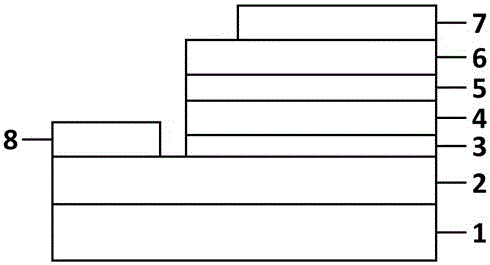
a ta 2 o 5 /zno/hfo 2 Asymmetric double-heterojunction light-emitting diode and preparation method thereof

A light-emitting diode and double heterojunction technology, which is applied in the field of nanomaterials and optoelectronic devices, can solve the problems affecting the luminous performance of the device, the luminous intensity is not high, and limit the practical application, so as to achieve the optimization of material preparation process, improve the luminous efficiency, and achieve good results. The effect of current spreading

Active Publication Date: 2016-08-17
WUHAN UNIV
View PDF7 Cites 0 Cited by
  • Summary
  • Abstract
  • Description
  • Claims
  • Application Information

AI Technical Summary

Problems solved by technology

Existing ZnO-based light-emitting diodes generally have problems such as low luminous intensity and excessive threshold current, which will cause the device to heat up and affect the stability and luminous performance of the device, which limits its practical application.

Method used


Image

  • a ta  <sub>2</sub> o  <sub>5</sub> /zno/hfo  <sub>2</sub> Asymmetric double-heterojunction light-emitting diode and preparation method thereof
  • a ta  <sub>2</sub> o  <sub>5</sub> /zno/hfo  <sub>2</sub> Asymmetric double-heterojunction light-emitting diode and preparation method thereof
  • a ta  <sub>2</sub> o  <sub>5</sub> /zno/hfo  <sub>2</sub> Asymmetric double-heterojunction light-emitting diode and preparation method thereof

Examples


Embodiment 1

[0023] 1. Substrate cleaning: Use p-type GaN grown on sapphire as the substrate, cut it into a size of 15mm×15mm, ultrasonically clean it with acetone, alcohol, and deionized water for 5 minutes, and finally dry it with a nitrogen gun.

[0024] 2. Ta 2 o 5 / ZnO / HfO 2 Growth of asymmetric double heterojunction: put the cleaned substrate into the growth chamber of the RF magnetron sputtering system, and pump the growth chamber to a background vacuum of 5×10 -4 Pa, the substrate is heated until its temperature reaches 200°C. Choose HfO 2 Ceramic target, ZnO ceramic target and Ta metal target were used as the preparation of HfO 2 thin film, intrinsic ZnO thin film and Ta 2 o 5 Thin film targets. Before coating each layer of film, it was pre-sputtered for 10 min to remove impurities on the target surface. Using the method of radio frequency magnetron sputtering, HfO is first deposited on the p-type GaN substrate 2 Thin film, the deposition substrate temperature is 200°C, ...

Embodiment 2

[0029] 1. Substrate cleaning: Use p-type GaN grown on sapphire as the substrate, cut it into a size of 15 mm×15 mm, ultrasonically clean it with acetone, alcohol, and deionized water for 5 minutes, and finally dry it with a nitrogen gun .

[0030] 2. Ta 2 o 5 / ZnO / HfO 2 Growth of asymmetric double heterojunction: put the cleaned substrate into the growth chamber of the RF magnetron sputtering system, and pump the growth chamber to a background vacuum of 1×10 -3 Pa, the substrate is heated until its temperature reaches 300°C. Choose HfO 2 Ceramic target, ZnO ceramic target and Ta metal target were used as the preparation of HfO 2 thin film, intrinsic ZnO thin film and Ta 2 o 5 Thin film targets. Before coating each layer of film, it was pre-sputtered for 10 min to remove impurities on the target surface. Using the method of radio frequency magnetron sputtering, HfO is first deposited on the p-type GaN substrate 2 Thin film, the deposition substrate temperature is 300...

Embodiment 3

[0035] 1. Substrate cleaning: Use p-type GaN grown on sapphire as the substrate, cut it into a size of 15 mm×15 mm, ultrasonically clean it with acetone, alcohol, and deionized water for 5 minutes, and finally dry it with a nitrogen gun .

[0036] 2. Ta 2 o 5 / ZnO / HfO 2 Growth of asymmetric double heterojunction: put the cleaned substrate into the growth chamber of the RF magnetron sputtering system, and pump the growth chamber to a background vacuum of 1×10 -3 Pa, the substrate is heated until its temperature reaches 300°C. Choose HfO 2 Ceramic target, ZnO ceramic target and Ta metal target were used as the preparation of HfO 2 thin film, intrinsic ZnO thin film and Ta 2 o 5 Thin film targets. Before coating each layer of film, it was pre-sputtered for 10 min to remove impurities on the target surface. Using the method of radio frequency magnetron sputtering, HfO is first deposited on the p-type GaN substrate 2 For thin film, the deposition substrate temperature is...


PUM


Abstract

The invention discloses a Ta2o5 / ZnO / HfO2 asymmetric double-heterojunction light emitting diode and a manufacturing method thereof. An HfO2 electronic barrier layer, an intrinsic ZnO active layer, a Ta2O5 hole barrier layer and a first electrode are sequentially arranged on a substrate of the light emitting diode from top to bottom; and a second electrode and the HfO2 electronic barrier layer are deposited on the substrate in parallel. Ta2O5 serves as the hole barrier layer; a current carrier is limited in the ZnO active layer by matching the hole barrier layer and the HfO2 electronic barrier layer; luminescence of a p-GaN substrate side can be effectively restrained; and the luminous intensity of the ZnO active layer is improved. The luminous peak wavelength of the Ta2O5 / ZnO / HfO2 asymmetric double-heterojunction light emitting diode is close to 680 nanometers, and the half-width of the Ta2O5 / ZnO / HfO2 asymmetric double-heterojunction light emitting diode is 150 nanometers. The Ta2O5 / ZnO / HfO2 asymmetric double-heterojunction light emitting diode is simple in manufacturing process and low in cost; and industrialization is easy to implement.

Description

technical field [0001] The present invention relates to a Ta 2 o 5 / ZnO / HfO 2 An asymmetrical double heterojunction light-emitting diode and a preparation method thereof belong to the field of nanometer materials and optoelectronic devices. Background technique [0002] Zinc oxide (ZnO) is a new type II-VI direct bandgap wide bandgap semiconductor material. The band gap of ZnO at room temperature is 3.37eV, and its exciton binding energy can reach 60meV, which is much higher than GaN's 25meV and room temperature thermal energy (26meV), so it is very suitable for making luminescent, photosensitive materials at room temperature or higher temperature. and other optoelectronic devices. The crystal structure and forbidden band width of ZnO are similar to those of GaN, but it has larger exciton binding energy and higher melting point than GaN. Good electromechanical coupling characteristics, thermal stability and chemical stability, combined with low cost and environmental fr...

Claims


Application Information

Patent Timeline
Patent Type & Authority Patents(China)
IPC IPC(8): H01L33/02H01L33/26H01L33/14
CPCH01L33/14H01L33/145H01L33/28
Inventor 方国家王皓宁龙浩李颂战莫小明陈昭
Owner WUHAN UNIV
Why Eureka
Try Eureka