Integrated circuit copper interconnection structure and preparation method thereof

A technology of copper interconnection structure and integrated circuit, which is applied in the field of microelectronics, can solve the problems such as the increase of characteristic aspect ratio, and achieve the effect of improving conductivity, reducing thickness and reducing resistivity

Inactive Publication Date: 2014-04-23
FUDAN UNIV
View PDF3 Cites 0 Cited by
  • Summary
  • Abstract
  • Description
  • Claims
  • Application Information

AI Technical Summary

Problems solved by technology

[0005]At present, the industry mainly adopts Magnetron Sputtering (Magnetron Sputtering) technology to prepare the diffusion barrier layer and Cu seed layer. However, as the feature size is further reduced, The thickness of the dielectric layer does not scale down accordingly, resulting in a larger feature aspect ratio

Method used


Image

  • Integrated circuit copper interconnection structure and preparation method thereof
  • Integrated circuit copper interconnection structure and preparation method thereof
  • Integrated circuit copper interconnection structure and preparation method thereof

Examples


Embodiment Construction
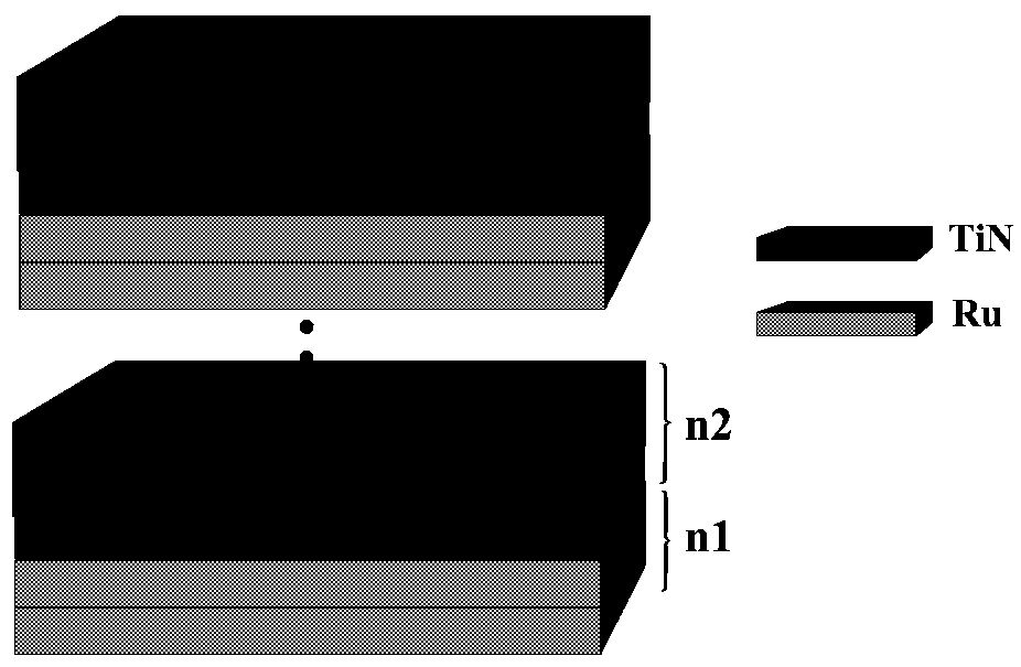
[0031] The basic idea of ​​the present invention is to use the ALD method to grow the overlapping structure of TiN and Ru atomic layers to form a Ru-N-Ti composite structure instead of the traditional TaN / Ta as the Cu diffusion barrier layer / adhesion layer / seed layer.

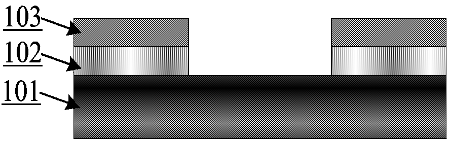
[0032] refer to figure 1 , using standard cleaning SC-1, SC-2 solution, 1:20 diluted hydrofluoric acid and deionized water to clean the Si substrate in sequence to remove impurities and natural oxide layer, and use high-purity N 2 blow dry. On the cleaned Si substrate (101), deposit the etch stop layer silicon nitride (102) and the dielectric layer SiO for interlayer insulation in sequence. 2 (103). The trenches or vias for the interconnect structure are formed using standard photolithography and etching processes.

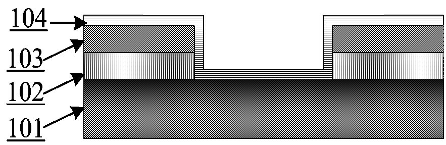
[0033] refer to figure 2 , growing Ru-N-Ti films on the trenches using PEALD technique (104). The TiN growth source is TDEAT and NH 3 Gas plasma, Ru growth source is Ru(Cp) 2 and O 2 plasm...


PUM

PropertyMeasurementUnit
thicknessaaaaaaaaaa

Abstract

The invention belongs to the technical field of micro electronics, and particularly relates to an integrated circuit copper interconnection structure and a preparation method thereof. A Ru-N-Ti structure is adopted to substitute a conventional TaN / Ta structure to act as a diffusion blocking layer / adhesive layer / seed crystal layer. An atomic layer deposition (ALD) film coating method is applied to prepare a Rux(TiN)y thin film, wherein a value range of x and y is 0.05-0.95, and the sum of x and y is 1. Proportion of Ru and TiN is adjusted so that excellent adhesive capability and diffusion blocking capability of Cu can be obtained. The amorphous thin film can be evenly grown on a structure with a high aspect ratio, and the acquired Ru-N-Ti structure can act as the diffusion blocking layer / adhesive layer / seed crystal layer of Cu so that technology steps and overall thickness of a thin film device can be reduced, diffusion blocking and adhesive performance of Cu can be improved and copper interconnection conductive performance can be enhanced.

Description

technical field [0001] The invention belongs to the technical field of microelectronics, and in particular relates to a novel integrated circuit copper interconnection structure based on atomic layer deposition (ALD) technology and a preparation method thereof. Background technique [0002] With the development of ultra-large-scale integrated circuits and ultra-large-scale integrated circuits, the integration of devices continues to increase, and the feature size of devices will decrease accordingly. Interconnect line delays replace device gate delays and become the main factor restricting the further improvement of IC speed. Due to the increased interconnection resistance R and parasitic capacitance C, the time constant RC of the interconnection is greatly increased, which causes the degradation of device performance. Chip interconnection becomes a key factor affecting chip performance. Copper (Cu) has a resistivity 35% lower than Al, 2 orders of magnitude higher than Al i...

Claims


Application Information

Patent Timeline
Patent Type & Authority Applications(China)
IPC IPC(8): H01L23/532H01L21/768
Inventor 卢红亮张远耿阳朱尚斌孙清清张卫
Owner FUDAN UNIV
Why Eureka
Try Eureka