Solar cell device and preparation method thereof
A solar cell and device technology, applied in the direction of electrical solid devices, semiconductor/solid device manufacturing, electrical components, etc., can solve the problems of low energy conversion efficiency of solar cells, improve photoelectric conversion efficiency, facilitate transmission, and energy conversion efficiency high effect
- Summary
- Abstract
- Description
- Claims
- Application Information
AI Technical Summary
Problems solved by technology
Method used
Image
Examples
preparation example Construction
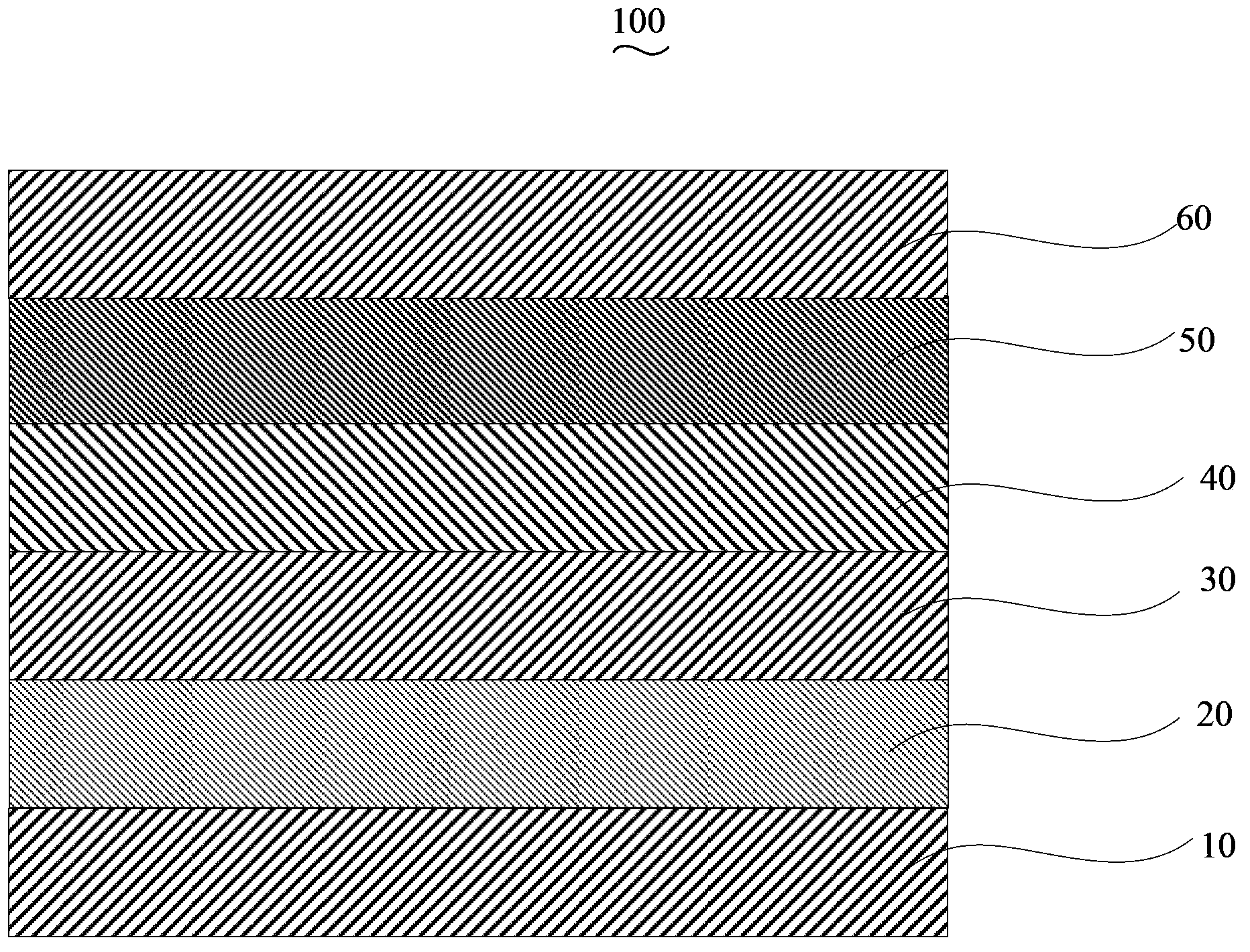
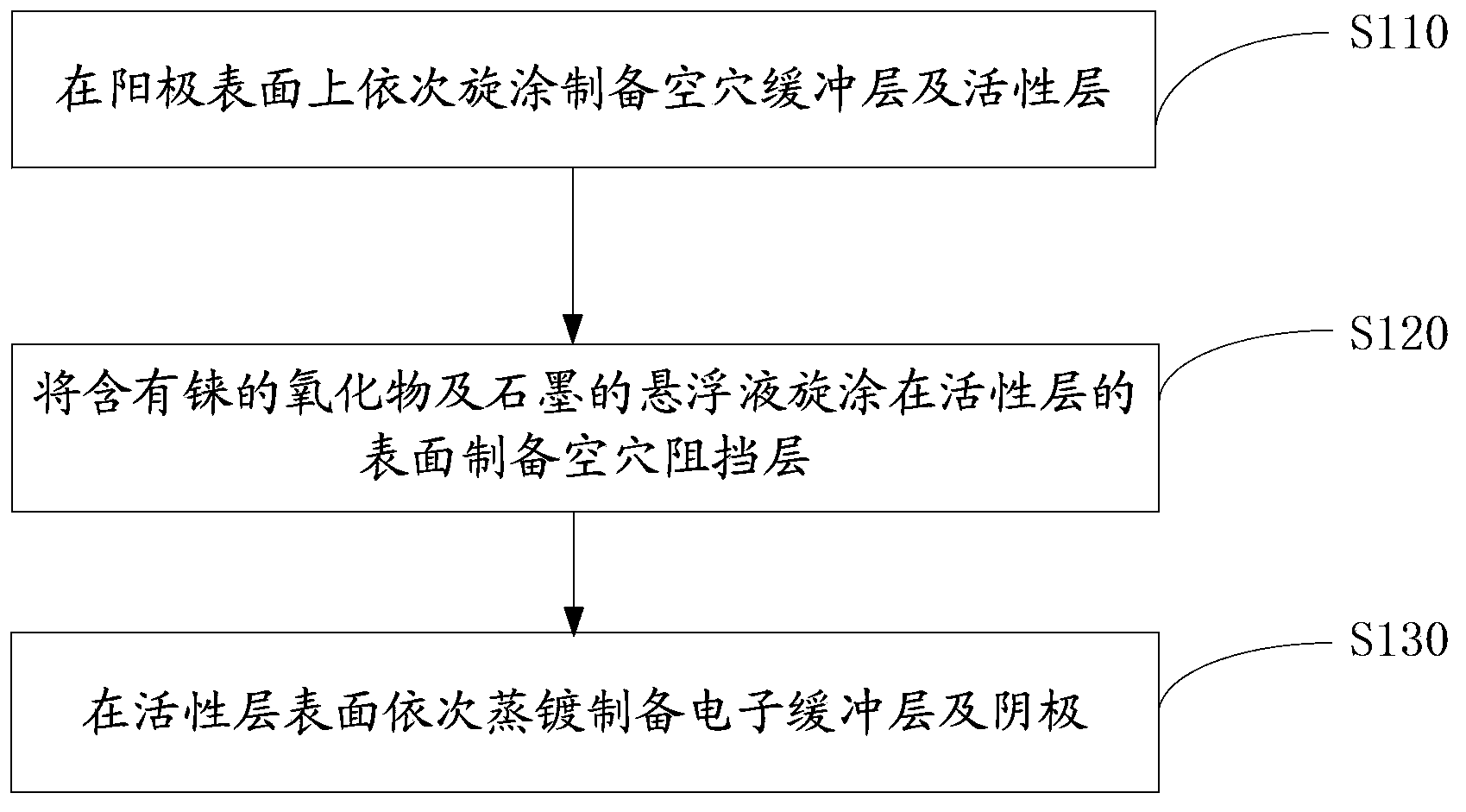
[0032] see also figure 2 , the preparation method of the solar cell device 100 of an embodiment, it comprises the following steps:
[0033] In step S110 , the hole buffer layer 20 and the active layer 30 are prepared by spin coating on the surface of the anode 10 in sequence.
[0034] The anode 10 is indium tin oxide glass (ITO), fluorine doped tin oxide glass (FTO), aluminum doped zinc oxide glass (AZO) or indium doped zinc oxide glass (IZO).
[0035] In this embodiment, the pretreatment of the anode 10 includes removing organic pollutants on the surface of the anode 10 and performing plasma oxygen ion treatment on the anode 10 . The anode 10 is ultrasonically cleaned with detergent, deionized water, acetone, ethanol, and isoacetone for 15 minutes each to remove the organic pollutants on the surface of the substrate 10; ~50W.
[0036] The hole buffer layer 20 is prepared by spin coating a solution containing a hole buffer material on the surface of the anode 10 . The rot...
Embodiment 1
[0047] The structure prepared in this example is ITO / PEDOT:PSS / P3HT:PCBM / Re 2 O 7 : Graphite / LiF / Al solar cell devices.
[0048] First, the ITO is subjected to photolithography, and then cut into the required size, and then ultrasonicated with detergent, deionized water, acetone, ethanol, and isopropanol for 15 minutes each to remove organic pollutants on the glass surface; after cleaning, the conductive substrate is cleaned. Carry out oxygen plasma treatment, the treatment time is 5-15min, and the power is 10-50W; on the above-mentioned substrate, spin-coating an aqueous solution of PEDOT:PSS with a mass fraction of 1.3% to prepare a hole buffer layer, and the mass ratio of PEDOT to PSS is 6: 1. The rotation speed of spin coating is 3000rpm and the time is 25s. After spin coating, heat at 200°C for 30 minutes, and the thickness of the hole buffer layer is 40nm. The solution is spin-coated, the solvent is chlorobenzene, the mass of P3HT and PCBM is 1:1, the spin-coating spee...
Embodiment 2
[0055] The structure prepared in this example is IZO / PEDOT:PSS / P3HT:PCBM / ReO 2 : Graphite / Cs 2 CO 3 / Au solar cell device.
[0056] First, the IZO is subjected to photolithography processing, cut into the required size, and then ultrasonicated with detergent, deionized water, acetone, ethanol, and isopropanol for 15 minutes each to remove organic pollutants on the glass surface; after cleaning, the conductive substrate is cleaned. Oxygen plasma treatment was carried out, the treatment time was 5-15min, and the power was 10-50W; the hole buffer layer was spin-coated, using a PEDOT:PSS aqueous solution with a weight ratio of 2:1, the mass fraction was 5%, and the spin-coating speed was 2000rpm , the time is 30s, after spin coating, it is heated at 200℃ for 15min, and the thickness is controlled at 80nm. The active layer was spin-coated, the material was P3HT:PCBM, the solvent was chloroform, the concentration was 24 mg / ml, the mass ratio was 1:4, the spin-coating speed was 40...
PUM
 Abstract
Description
Claims
Application Information


