Nitride LED epitaxy structure suitable for heavy current driving

An epitaxial structure and nitride technology, applied in circuits, electrical components, semiconductor devices, etc., can solve problems such as reducing the probability of the overlap of electron and hole wave functions, uneven distribution of carrier concentration and recombination, and adverse effects on quantum efficiency. , to weaken the adverse effects, improve the internal quantum efficiency of the LED, and reduce the intensity of the built-in polarization electric field

Inactive Publication Date: 2014-06-11
TONGFANG OPTO ELECTRONICS +1
View PDF3 Cites 8 Cited by
  • Summary
  • Abstract
  • Description
  • Claims
  • Application Information

AI Technical Summary

Problems solved by technology

Quantum wells with energy band bending will reduce the coincidence probability of electron and hole wave functions, thereby reducing quantum efficiency
⑵Crystal defects and leakage phenomenon
The higher density of crystal defects in nitride crystals is a ubiquitous problem, which is both the physical path for leakage current transport/conduction and the existence of non-radiative transition cente

Method used


Image

  • Nitride LED epitaxy structure suitable for heavy current driving
  • Nitride LED epitaxy structure suitable for heavy current driving
  • Nitride LED epitaxy structure suitable for heavy current driving

Examples


Embodiment 1

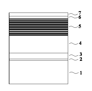
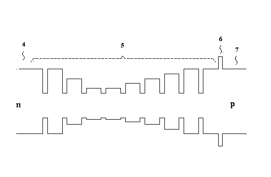
[0030] see figure 1 , the present invention is sapphire substrate 1, GaN low-temperature buffer layer 2, non-doped GaN layer 3, n-type GaN electron injection layer 4, composed of 10 In x Ga 1-x N (0≤x≤1) quantum barrier and 9 In 0.2 Ga 0.8 Active region layer 5 composed of N quantum wells, Al 0.13 Ga 0.87 N p-type electron blocking layer 6 and p-type GaN hole injection layer 7 . Among them, the film thickness of the GaN low-temperature buffer layer 2 is 25nm; the thickness of the non-doped GaN layer 3 is 2.5 μm; the thickness of the n-type GaN electron injection layer 4 is 2.5 μm, and a 5×10 19 / cm 3 concentration of Si for n-type doping. 10 In x Ga 1-xThe x values ​​of N (0≤x≤1) quantum barriers are 0, 0, 0.06, 0.14, 0.14, 0.12, 0.06, 0.03, 0, 0 from bottom to top, that is, the forbidden band width of quantum barriers decreases first. Small and then increase the change trend, the film thickness of the quantum barrier remains unchanged at 10nm. The forbidden band w...

Embodiment 2

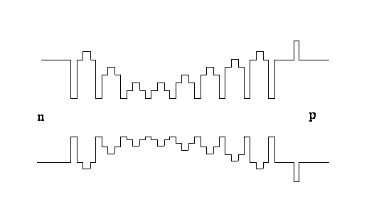
[0032] Except for the active region layer 5 , the LED epitaxial structure of Embodiment 2 of the present invention is completely the same as that of Embodiment 1. Such as image 3 , the active region 5 consists of 10 In x Ga 1-x N / Al y In z Ga 1-y-z N / In x Ga 1-x N (0≤x≤1; 0≤y, z≤1; y+z≤1) quantum barrier and 9 In 0.2 Ga 0.8 N quantum well composition. Among them, the single quantum barrier In x Ga 1-x N / Al y In z Ga 1-y-z N / In x Ga 1-x N consists of three layers of nitride In x Ga 1-x N. Al y In z Ga 1-y-z N, In x Ga 1-x N composition. In the same quantum barrier, the chemical composition of the first and third layers of nitride is the same, and the band gap of the second layer of nitride is larger than that of the other two layers. If the ordered real number pair (x, y, z) is used to represent the material composition of a single quantum barrier trilayer nitride, then, with the above 10 quantum barriers In x Ga 1-x N / Al y In z Ga 1-y-z N / In ...

Embodiment 3

[0034] Except for the active region 5, the epitaxial structure of the LED in the third embodiment of the present invention is completely the same as that in the first embodiment. see Figure 4 , the active region 5 consists of 8 In x Ga 1-x N (0≤x≤1) quantum barrier and 7 In 0.2 Ga 0.8 N quantum well composition. According to the bottom-up sequence of epitaxial growth, 8 In x Ga 1-x The maximum forbidden band width of N (0≤x≤1) quantum barriers shows a trend of decreasing first and then increasing. Among them, the material of the first and eighth quantum barriers is GaN; the forbidden band width of the second and third quantum barriers shows a uniformly decreasing change mode, and the value of x representing their chemical composition increases uniformly from 0 to 0.03, uniformly increased from 0.06 to 0.09; the forbidden band widths of the 4th, 5th, 6th, and 7th quantum barriers showed a uniform increase, and their x values ​​were uniformly decreased from 0.15 to 0.12,...


PUM

PropertyMeasurementUnit
Film thicknessaaaaaaaaaa
Thicknessaaaaaaaaaa
Thicknessaaaaaaaaaa

Abstract

The invention discloses a nitride LED epitaxy structure suitable for heavy current driving, and relates to the technical field of manufacturing of LED optoelectronic devices. According to the structure of the nitride LED epitaxy structure suitable for heavy current driving, a substrate sequentially comprises an n-type compound semiconductor, an active area and a p-type compound semiconductor from bottom to top, and is characterized in that the active area is formed by alternatively overlapping m quantum wells and m+1 quantum barriers, the m is any natural number, the maximum forbidden band gap of the quantum barriers is larger than the maximum forbidden band gap of the adjacent quantum wells, and the maximum forbidden band gap or film layer thickness of different quantum barriers is distributed in a gradual variation mode. Compared with the prior art, the nitride LED epitaxy structure suitable for heavy current driving can reduce or eliminate the problem of decrease of the energy efficiency of nitride LEDs under the condition of heavy current driving, and improve the quantum efficiency of devices.

Description

technical field [0001] The invention relates to the technical field of manufacturing LED optoelectronic devices, in particular to a nitride LED epitaxial growth structure suitable for high-current driving. Background technique [0002] Al nitride based x In y Ga 1-x-y N (0≤x, y≤1; x+y≤1; wurtzite crystal structure) Light-emitting diode LEDs made of semiconductor materials are gradually used in electronic display screens, landscape lighting, miner's lamps, and street lamps due to their advantages in energy saving, environmental protection, and long life. , LCD backlight, general lighting, biomedicine and other fields are widely used. Due to nitride Al x In y Ga 1-x-y The wide bandgap of N (0≤x, y≤1; x+y≤1) semiconductors is approximately in the range of 1.9-6.2 eV, which just covers the spectral energy range from yellow-green light to ultraviolet light. The emission wavelength of the LED device can be precisely formulated by controlling the cation composition of the n...

Claims


Application Information

Patent Timeline
IPC IPC(8): H01L33/06H01L33/32
CPCH01L33/06H01L33/02H01L33/32
Inventor 马亮梁信伟
Owner TONGFANG OPTO ELECTRONICS
Why Eureka
Try Eureka