LED epitaxial wafer grown on Si substrate and preparation method thereof

An LED epitaxial wafer and substrate technology, applied in semiconductor/solid-state device manufacturing, electrical components, circuits, etc., can solve problems such as epitaxial wafer cracking, reducing LED luminous efficiency, affecting GaN growth quality, etc. The effect of smooth transition of transition and prevention of AlN quality degradation

Active Publication Date: 2014-09-10
广州市众拓光电科技有限公司
View PDF3 Cites 34 Cited by
  • Summary
  • Abstract
  • Description
  • Claims
  • Application Information

AI Technical Summary

Problems solved by technology

However, the quality of GaN single crystal thin films prepared on Si substrates is not as good as that of sapphire substrates, mainly due to: the thermal mismatch between Si and GaN is much higher than that of sapphire, which makes epitaxial wafers more prone to cracking; Amorphous SixNy is easy to form at the interface, which affects the growth quality of GaN; the absorption of visible light by Si will also greatly reduce the luminous efficiency of LED

Method used


Image

  • LED epitaxial wafer grown on Si substrate and preparation method thereof
  • LED epitaxial wafer grown on Si substrate and preparation method thereof
  • LED epitaxial wafer grown on Si substrate and preparation method thereof

Examples


Embodiment 1

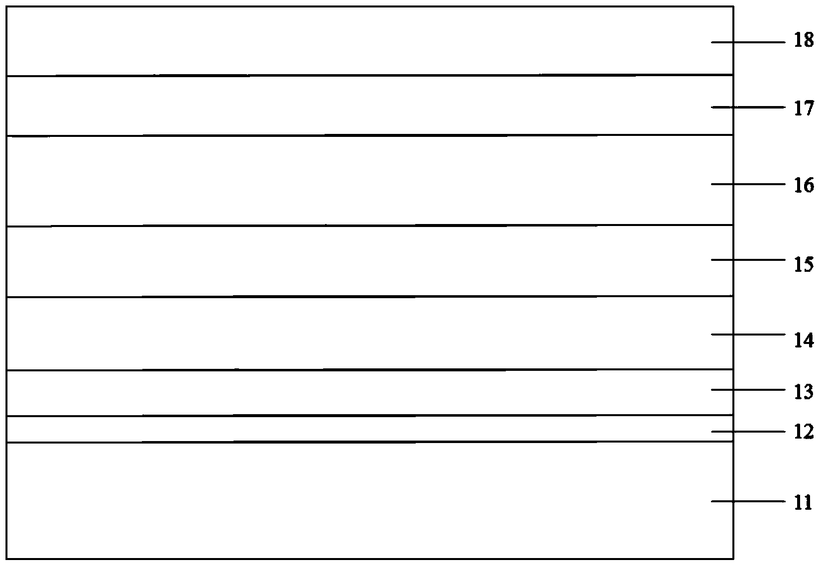
[0037] Please refer to figure 1, the LED epitaxial wafer grown on the Si substrate of the present invention comprises a Si substrate 11, a first AlN buffer layer 12, a second AlN buffer layer 13, an AlGaN step buffer layer 14, a u-GaN layer 15, an n-GaN Layer 16, InGaN / GaN quantum well layer 17 and p-GaN layer 18;

[0038] The above-mentioned LED epitaxial wafer grown on the Si substrate is obtained by the following method:

[0039] (1) Selection of the substrate and its crystal orientation: a Si substrate is used, and the crystal orientation of the (111) plane offset by 0.5° to the (100) direction is selected.

[0040] (2) The first AlN buffer layer is grown by pulsed laser deposition process. The process conditions are as follows: substrate temperature is 650°C, reaction chamber pressure is 1mTorr, V / III ratio is 30, growth rate is 0.5ML / s, and the first AlN The thickness of the buffer layer was 20 nm.

[0041] (3) The second AlN buffer layer was grown by the metal-organi...

Embodiment 2

[0049] The characteristics of this embodiment are:

[0050] The LED epitaxial wafer grown on the Si substrate is obtained by the following method:

[0051] (1) Selection of the substrate and its crystal orientation: a Si substrate is used, and the crystal orientation of the (111) plane offset by 1° to the (100) direction is selected.

[0052] (2) The first AlN buffer layer is grown by the pulsed laser deposition process. The process conditions are as follows: the substrate temperature is 850°C, the reaction chamber pressure is 10mTorr, the V / III ratio is 45, the growth rate is 0.6ML / s, and the first AlN The thickness of the buffer layer was 10 nm.

[0053] (3) The second AlN buffer layer was grown by the metal-organic chemical vapor deposition process. The process conditions were as follows: the substrate temperature was 960 ° C, the reaction chamber pressure was 100 Torr, the V / III ratio was 2500, and the growth rate was 0.1 μm / h. The thickness of the second AlN buffer laye...

Embodiment 3

[0061] This embodiment is modified on the basis of embodiment 1, the difference is that: before growing the AlN buffer layer, the substrate is subjected to surface cleaning and annealing steps in sequence, the specific method is as follows:

[0062] Surface cleaning treatment: ultrasonically clean the Si substrate in acetone solution first, then ultrasonically clean in deionized water; then ultrasonically clean in isopropanone solution; then ultrasonically clean in hydrofluoric acid solution, and then Soak in water; then soak the Si substrate in a mixed solution of sulfuric acid and hydrogen peroxide; finally soak the Si substrate in hydrofluoric acid, rinse with deionized water, and blow dry with nitrogen.

[0063] Annealing treatment: bake the substrate at a high temperature of 900-1000° C. for 3-5 hours.

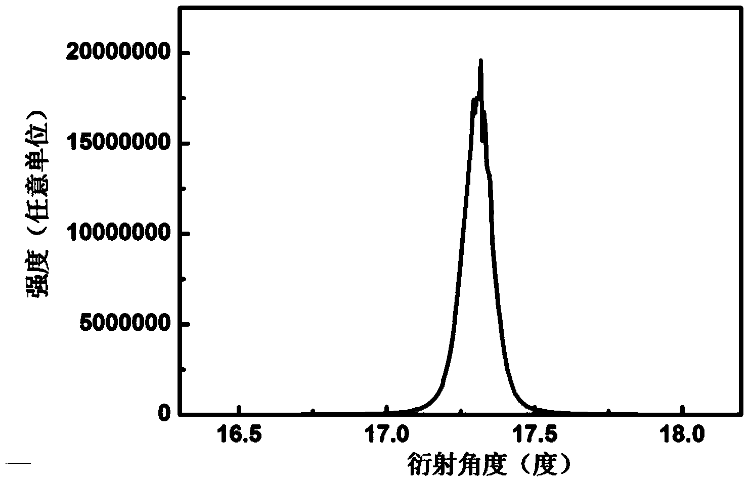
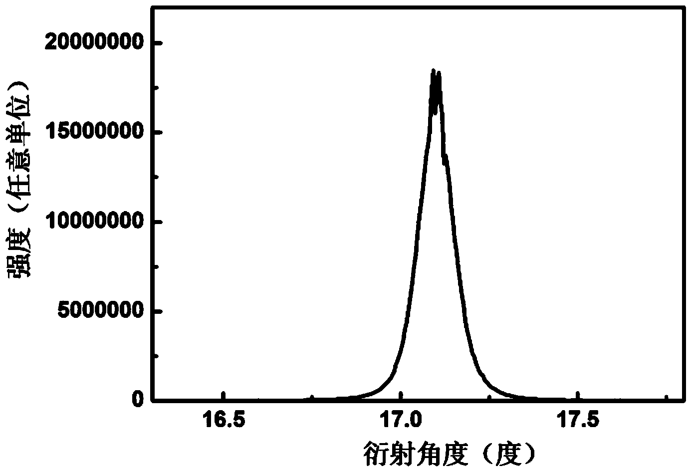
[0064] Please refer to Figure 4 , it can be seen from the X-ray pendulum curve that the half-maximum width (FWHM) value of GaN(002) in the LED epitaxial wafer is 375arc...


PUM

PropertyMeasurementUnit
thicknessaaaaaaaaaa
thicknessaaaaaaaaaa
thicknessaaaaaaaaaa

Abstract

The invention discloses an LED epitaxial wafer grown on an Si substrate and a preparation method thereof. The LED epitaxial wafer grown on the Si substrate is prepared through the following preparation method: using the Si substrate, enabling the surface (111) of the Si substrate to deviate from (100) by 0.5 to 1 degree, growing a first AlN buffer layer, and growing a second AlN buffer layer, an AlGaN step buffer layer, a u-GaN layer, an n-GaN layer, an InGaN/GaN quantum well layer and a p-GaN layer in sequence. The LED epitaxial wafer grown on the Si substrate uses Si as the substrate, the preparation method combines a metal organic chemical vapor deposition technique and a pulsed laser deposition technique, a procedure of pre-paving Al for using the metal organic chemical vapor deposition technique to grow the AlN is omitted, the problem that Si is diffused to the AlN buffer layer under a high temperature to damage the surface shape is avoided, and the LED epitaxial wafer is good in performance, high in crystal quality and suitable for LED devices.

Description

technical field [0001] The invention relates to an LED epitaxial wafer, in particular to an LED epitaxial wafer grown on a Si substrate and a preparation method thereof. Background technique [0002] LED is a product under the social background of advocating energy saving and emission reduction. It has good environmental protection, energy saving and anti-seismic performance, and has broad prospects in the future lighting market. It is known as the fourth-generation green lighting source. [0003] As one of the representatives of the third-generation semiconductor materials, GaN has excellent properties such as direct band gap, wide band gap, high saturation electron drift velocity, high breakdown electric field, and high thermal conductivity, and has attracted extensive attention in microelectronic applications. Since I. Akasaki successfully obtained p-GaN for the first time and achieved a new breakthrough in blue LEDs, GaN-based compounds have been the main materials for p...

Claims


Application Information

Patent Timeline
Patent Type & Authority Applications(China)
IPC IPC(8): H01L33/12H01L33/16H01L33/00
CPCH01L21/02381H01L21/02458H01L21/0254H01L21/0262H01L33/0066H01L33/0075H01L33/12H01L33/16H01L33/32
Inventor 李国强
Owner 广州市众拓光电科技有限公司
Why Eureka
Try Eureka