Light-emitting diode (LED) epitaxial wafer growing on Si patterned substrate and preparation process of LED epitaxial wafer

A technology of LED epitaxial wafers and graphic substrates, which is applied in semiconductor/solid-state device manufacturing, electrical components, circuits, etc., can solve problems affecting the growth quality of GaN, epitaxial wafer cracks, and reduce LED luminous efficiency, etc., to avoid light absorption difficulties , Promote lateral epitaxial growth, and improve crystal quality

Active Publication Date: 2014-09-10
广州市众拓光电科技有限公司
View PDF10 Cites 10 Cited by
  • Summary
  • Abstract
  • Description
  • Claims
  • Application Information

AI Technical Summary

Problems solved by technology

However, the quality of GaN single crystal thin films prepared on Si patterned substrates is not as good as that of sapphire substrates, mainly due to: the thermal mismatch between Si and GaN is much higher than that of sapphire, which makes epitaxial wafers more prone to cracking; N is easy to form amorphous SixNy at the interface, which affects the growth quality of GaN; the absorption of visible light by Si will also greatly reduce the luminous efficiency of LED

Method used


Image

  • Light-emitting diode (LED) epitaxial wafer growing on Si patterned substrate and preparation process of LED epitaxial wafer
  • Light-emitting diode (LED) epitaxial wafer growing on Si patterned substrate and preparation process of LED epitaxial wafer
  • Light-emitting diode (LED) epitaxial wafer growing on Si patterned substrate and preparation process of LED epitaxial wafer

Examples


Embodiment 1

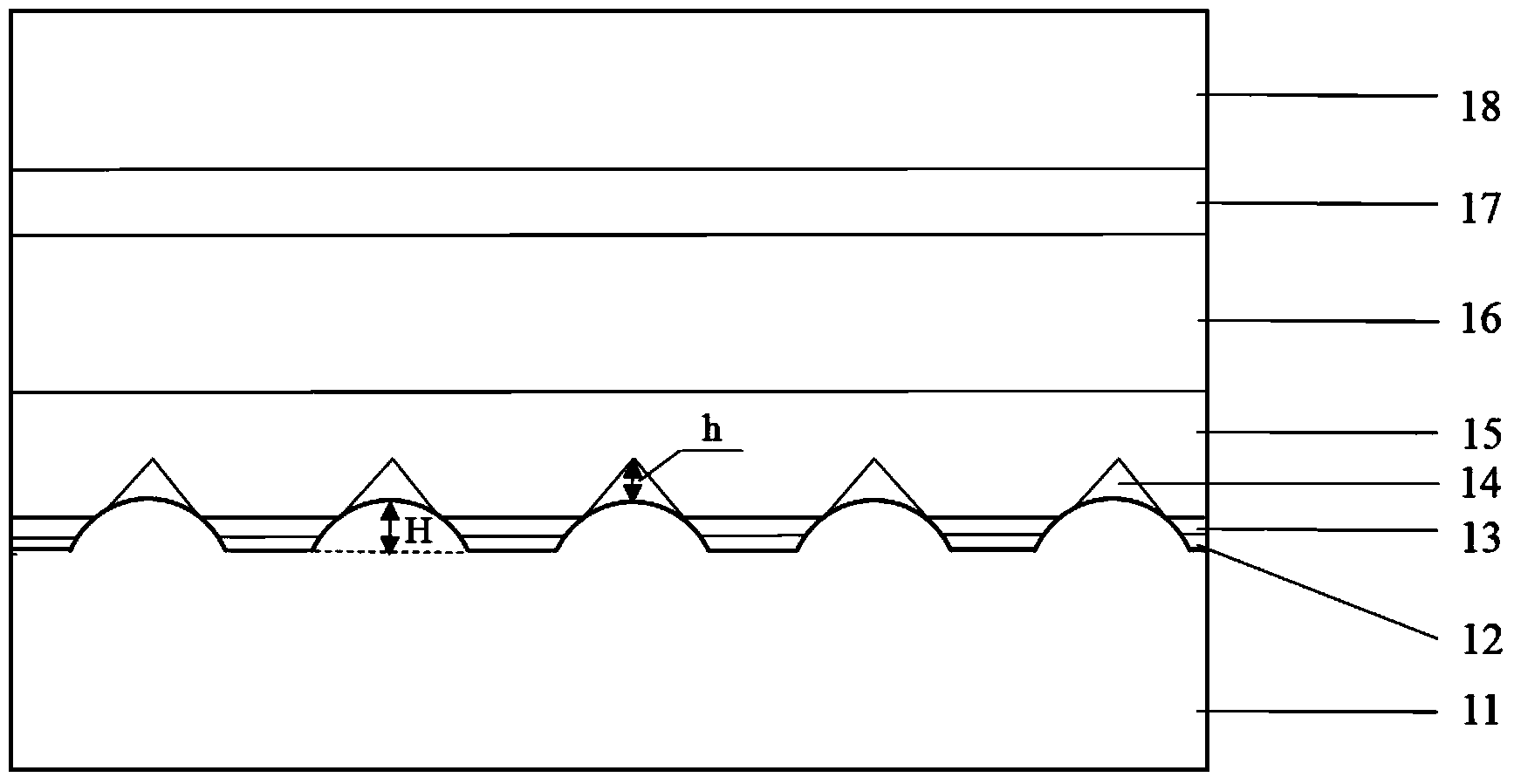
[0044] Please refer to Figure 1-Figure 3 , a kind of LED epitaxial wafer grown on the Si pattern substrate of the present invention, it comprises Si pattern substrate 11, the crystal orientation of described Si pattern substrate 11 is (111), is distributed with several identical shapes Pattern bump 11-1; AlN buffer layer 12, AlGaN step buffer layer 13, u-GaN layer 15, n-GaN layer 16, InGaN / GaN quantum well layer 17 are sequentially grown on the Si pattern substrate 11 and a p-GaN layer 18; a cavity 14 is formed on the top of each patterned protrusion 11-1.

[0045] The graphic protrusions 11-1 are in the shape of a hemisphere, the height H of the hemisphere is 1 μm, the side distance d is 1 μm, and the bottom width w is 1.5 μm; the arrangement is rectangular.

[0046] The above-mentioned LED epitaxial wafer grown on the Si pattern substrate is obtained by the following method:

[0047] (1) Selection of the substrate and its crystal orientation: a Si pattern substrate is use...

Embodiment 2

[0058] The characteristics of this embodiment are:

[0059] The LED epitaxial wafer grown on the Si pattern substrate is obtained by the following method:

[0060] (1) Selection of the substrate and its crystal orientation: a Si pattern substrate is used, and the (111) plane is selected.

[0061] (2) A 20nm-thick AlN buffer layer was grown by metal-organic chemical vapor deposition. The process conditions were: substrate temperature 960°C, reaction chamber pressure 100Torr, V / III ratio 3500, growth rate 0.3μm / h.

[0062] (3) AlGaN stepping buffer layer was grown by metal-organic chemical vapor deposition process. 3 The flow rate is 15slm, the TMAl flow rate is 250 sccm, the TMGa flow rate is 8 sccm, the growth rate is 0.2 μm / h, and the first AlGaN layer is grown with a thickness of 110 nm, and the Al doping amount is 80%; the TMGa flow rate is 25 sccm, and the growth rate is 0.4 μm / h, grow the second AlGaN layer with a thickness of 160nm, and the doping amount of Al is 60%; ...

Embodiment 3

[0071] This embodiment is modified on the basis of Embodiment 1, the difference is:

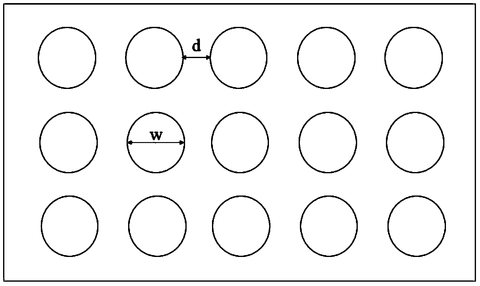
[0072] Please refer to Figure 5 , a plurality of cones with the same shape are arranged on the Si pattern substrate of the present invention, the height H of the cones is 1 μm, the side distance d is 1 μm, and the bottom width w is 1.5 μm; the arrangement is hexagonal.

[0073] Before growing the AlN buffer layer, the substrate is sequentially cleaned and annealed. The specific method is as follows:

[0074] Surface cleaning treatment: ultrasonically clean the Si pattern substrate in acetone solution first, then ultrasonically clean in deionized water; then ultrasonically clean in isopropanone solution; then ultrasonically clean in hydrofluoric acid solution, and then Soak in deionized water; then soak the Si pattern substrate in a mixed solution of sulfuric acid and hydrogen peroxide; finally soak the Si pattern substrate in hydrofluoric acid, rinse with deionized water, and blow dry with ...


PUM

PropertyMeasurementUnit
thicknessaaaaaaaaaa
thicknessaaaaaaaaaa
thicknessaaaaaaaaaa

Abstract

The invention discloses a light-emitting diode (LED) epitaxial wafer growing on an Si patterned substrate and a preparation process of the LED epitaxial wafer. The preparation process includes the following steps of using the Si patterned substrate and selecting a crystal face (111) as a crystal orientation, wherein a plurality of pattern projections with the same shapes are distributed on the crystal face (111); subsequently, sequentially growing an AlN buffer layer, an AlGaN step buffer layer, an u-GaN layer, an n-GaN layer, an InGaN/GaN quantum well layer and a p-GaN layer on the Si patterned substrate; finally, manufacturing a cavity in the top of each pattern projection. According to the LED epitaxial wafer growing on the Si patterned substrate and the preparation process of the LED epitaxial wafer, Si is used as the substrate, meanwhile, horizontal epitaxial growth of a thin film is promoted by combining the pattern substrate and the cavities, crystal qualities are improved, the stress condition is effectively relieved so as to solve the crack problem and avoid difficulties of light absorption of the Si patterned substrate, and the obtained LED epitaxial wafer is good in photoelectric property, high in crystalline quality, and applicable to LED devices.

Description

technical field [0001] The invention relates to an LED epitaxial wafer, in particular to an LED epitaxial wafer grown on a Si pattern substrate and a preparation method thereof. Background technique [0002] LED is a product under the social background of advocating energy saving and emission reduction. It has good environmental protection, energy saving and anti-seismic performance, and has broad prospects in the future lighting market. It is known as the fourth-generation green lighting source. [0003] As one of the representatives of the third-generation semiconductor materials, GaN has excellent properties such as direct band gap, wide band gap, high saturation electron drift velocity, high breakdown electric field, and high thermal conductivity, and has attracted extensive attention in microelectronic applications. Since I. Akasaki successfully obtained p-GaN for the first time and achieved a new breakthrough in blue LEDs, GaN-based compounds have been the main materia...

Claims


Application Information

Patent Timeline
Patent Type & Authority Applications(China)
IPC IPC(8): H01L33/22H01L33/12H01L33/00
CPCH01L21/02381H01L21/02458H01L21/0254H01L21/0262H01L33/0066H01L33/0075H01L33/12H01L33/22H01L33/32
Inventor 李国强
Owner 广州市众拓光电科技有限公司
Why Eureka
Try Eureka