Preparation method of TiO2/SnO2 semiconductor two-layer composite film photo anode

A double-layer composite and semiconductor technology, which is applied in coating, metal material coating technology, ion implantation plating, etc., can solve the problems of inability to effectively exert the metal photogenerated cathodic protection effect, unstable film bonding, and low photoelectric efficiency of the film, etc. problem, to achieve the effect of improving photogenerated cathodic protection effect, novel method and uniform film layer

Active Publication Date: 2014-09-17
XIAMEN UNIV
View PDF3 Cites 12 Cited by
  • Summary
  • Abstract
  • Description
  • Claims
  • Application Information

AI Technical Summary

Problems solved by technology

[0018] The purpose of the present invention is to overcome single TiO 2 The photoelectric efficiency of the thin film is low, the photo-generated cathodic protection effect on the metal cannot be effectively exerted in the dark state, and the combination of the composite film layer is unstable, etc., providing TiO with high-efficiency photo-generated cathodic protection effect 2 / SnO 2 Preparation method of semiconductor double-layer composite film photoanode

Method used


Image

  • Preparation method of TiO2/SnO2 semiconductor two-layer composite film photo anode
  • Preparation method of TiO2/SnO2 semiconductor two-layer composite film photo anode
  • Preparation method of TiO2/SnO2 semiconductor two-layer composite film photo anode

Examples


Embodiment 1

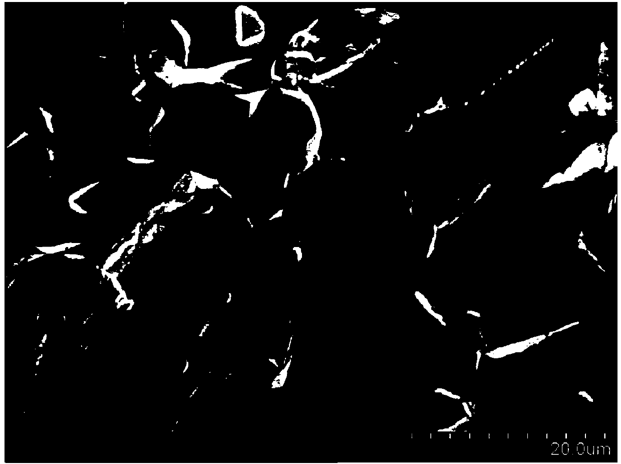
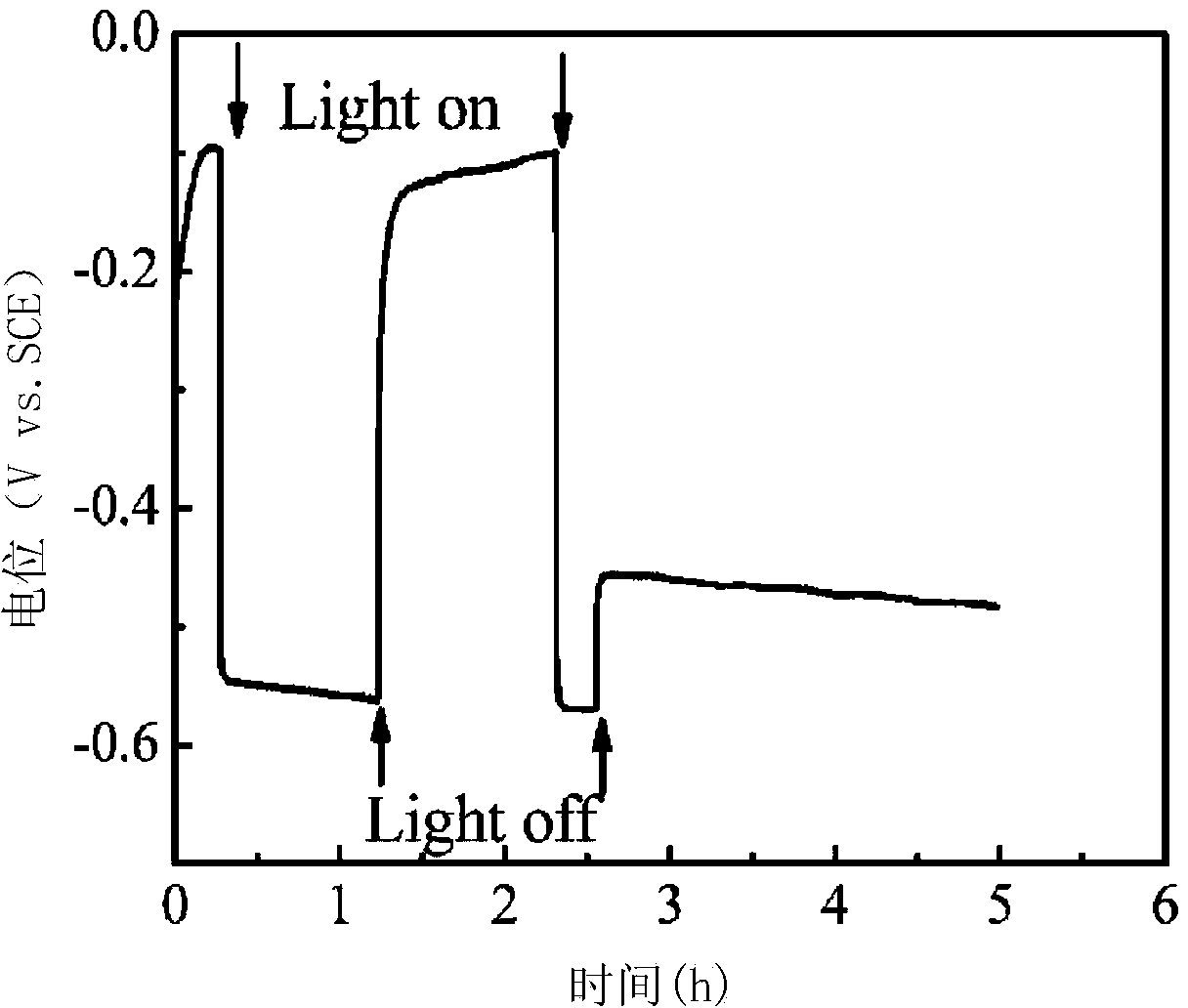
[0039] According to the above technical scheme, nano-TiO was prepared on the surface of 304 stainless steel 2 / SnO 2 Semiconductor double-layer composite film, and test the photogenerated cathodic protection effect of the film as a photoanode on 304 stainless steel.

[0040] A rectangular 304 stainless steel with a thickness of 0.2 mm is used as a sample, which is 1.5 cm long and 1.0 cm wide. The surface of the sample was polished with 800-1500 water-grinding paper and Al 2 o 3 After the polishing powder is polished, it is ultrasonically cleaned in acetone, absolute ethanol and deionized water for 10 min respectively.

[0041] Weigh 4.152g SnCl 2 2H 2 O, add 400mL ion water, dissolve and then add 4.248g NaNO 3 and 30 mL of concentrated HNO 3 Solution, after stirring, add deionized water to make the volume to 1000mL. That is to prepare a certain concentration of electrodeposition solution for use. Use DJS-292C potentiostat at room temperature, use platinum as auxiliary...

Embodiment 2

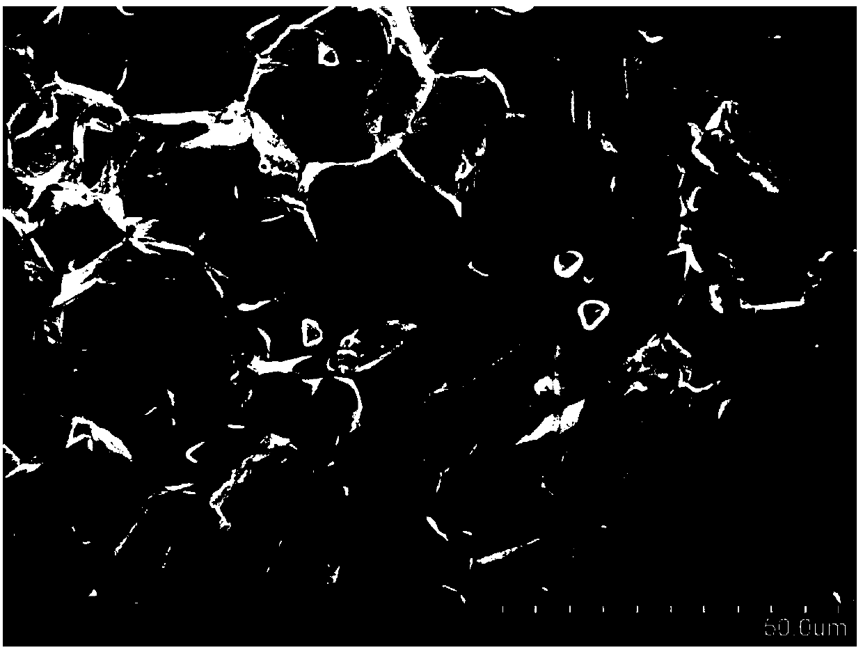
[0046] According to the above technical scheme, nano-TiO was prepared on the surface of 304 stainless steel 2 / SnO 2 Semiconductor double-layer composite film, and test the photogenerated cathodic protection effect of the film as a photoanode on 304 stainless steel.

[0047] A rectangular 304 stainless steel with a thickness of 0.2 mm is used as a sample, which is 1.5 cm long and 1.0 cm wide. After the surface of the sample was polished by No. 800-1500 water abrasive paper, it was ultrasonically cleaned in acetone, absolute ethanol and deionized water for 10 minutes respectively.

[0048] Weigh 4.152g SnCl 2 2H 2 O, add 400mL ion water, dissolve and then add 4.248g NaNO 3 and 30 mL of concentrated HNO 3 Solution, after stirring, add deionized water to make the volume to 1000mL. That is to prepare a certain concentration of electrodeposition solution for use. Use DJS-292C potentiostat at room temperature, use platinum as auxiliary electrode, calomel electrode as referenc...


PUM

PropertyMeasurementUnit
lengthaaaaaaaaaa
widthaaaaaaaaaa
thicknessaaaaaaaaaa

Abstract

The invention relates to a preparation method of a TiO2/SnO2 semiconductor two-layer composite film photo anode and relates to a semiconductor photo anode. The invention provides the preparation method of the TiO2/SnO2 semiconductor two-layer composite film photo anode with an efficient photo-induced cathodic protection effect. The preparation method comprises the following steps: 1) by using stainless steel as a matrix sample, grinding the surface of the matrix sample to a mirror surface, and then cleaning; 2) dissolving SnCl2.2H2O in water, then adding NaNO3 and nitric acid to prepare an electrolyte solution, and then adding water to fix the volume to 1000mL; by using platinum as a counter electrode and saturated mercurous chloride as a reference electrode and the matrix sample as a working electrode, in the electrolyte solution, electro-depositing and drying, namely electro-depositing a SnO2 film layer on the surface of the matrix sample; and 3) sputtering a TiO2 film on the surface of the SnO2 film layer obtained in the step 2), and then thermally treating to obtain the TiO2/SnO2 semiconductor two-layer composite film photo anode. The photo-induced cathodic protection effect on metals by a TiO2 nano thin film in dark state is improved.

Description

technical field [0001] The invention relates to a semiconductor photoanode, in particular to a TiO with high-efficiency photogenerated cathodic protection effect on stainless steel 2 / SnO 2 The invention discloses a method for preparing a semiconductive bilayer composite film photoanode. Background technique [0002] Photogenerated cathodic protection technology is the use of nano-TiO 2 The photoelectric conversion properties of the coating protect the metal, that is, TiO under light irradiation 2 Photogenerated electron-hole pairs are generated on the surface of the semiconductor, and the photogenerated electrons are transferred to the protected metal, reducing the electrode potential of the metal to significantly lower than its natural corrosion potential, making it cathodically polarized and protected [1-4] . However, due to TiO 2 The bandgap (E g ) is wide and can only absorb ultraviolet radiation accounting for about 5% of the solar spectrum, so the solar energy c...

Claims


Application Information

Patent Timeline
Patent Type & Authority Applications(China)
IPC IPC(8): C25D9/10C23C14/34C23C14/08C23F17/00
Inventor 杜荣归漆海清朱燕峰胡娟林昌健
Owner XIAMEN UNIV
Why Eureka
Try Eureka