
Organic electroluminescent device light-emitting layer, manufacturing method of organic electroluminescent device light-emitting layer and application of organic electroluminescent device light-emitting layer

A technology of electroluminescent devices and light-emitting layers, which is applied in the fields of electric solid-state devices, semiconductor/solid-state device manufacturing, electrical components, etc., and can solve problems such as ligand dissociation and unfavorable device performance.

Active Publication Date: 2014-10-01
厦门奥德生物科技有限公司
View PDF2 Cites 2 Cited by
  • Summary
  • Abstract
  • Description
  • Claims
  • Application Information

AI Technical Summary

Problems solved by technology

However, the possible ligand dissociation of metal complexes in the solution state is not conducive to achieving high device performance

Method used


Image

  • Organic electroluminescent device light-emitting layer, manufacturing method of organic electroluminescent device light-emitting layer and application of organic electroluminescent device light-emitting layer
  • Organic electroluminescent device light-emitting layer, manufacturing method of organic electroluminescent device light-emitting layer and application of organic electroluminescent device light-emitting layer
  • Organic electroluminescent device light-emitting layer, manufacturing method of organic electroluminescent device light-emitting layer and application of organic electroluminescent device light-emitting layer

Examples


Embodiment 1

[0084] Synthesis of host material Czpzpy

[0085]

[0086] (1) Synthesis of intermediate Brpzpy: Dissolve pyrazole (20mmol, 1.36g) in 1,4-dioxane (60mL), add potassium tert-butoxide (22mmol, 2.47g) and 2,6-dioxane in sequence Bromopyridine (20mmol, 4.74g). The reaction mixture was stirred at reflux for 48 hours and then quenched with 10 mL of water. After spin-drying the organic solvent, 300 mL of water was added to the reaction mixture and extracted several times with dichloromethane. The organic phases were combined, washed several times with saturated brine and dried over anhydrous sodium sulfate. The solvent was spin-dried and passed through the column to obtain a white solid Brpzpy (3.8 g, yield: 85%). Utilize nuclear magnetic resonance spectrometer to carry out analysis, the result is as follows: 1 H NMR (400MHz, CDCl 3 ): δ8.54(d, J=2.6Hz, 1H), 7.93(d, J=8.1Hz, 1H), 7.74(s, 1H), 7.66(t, J=7.9Hz, 1H), 7.36(d , J=7.7Hz, 1H), 6.47(s, 1H).

[0087] (2) Synthesis of...

Embodiment 2

[0090] Guest complex [Cu(Czpzpy)(POP)]BF 4

[0091]

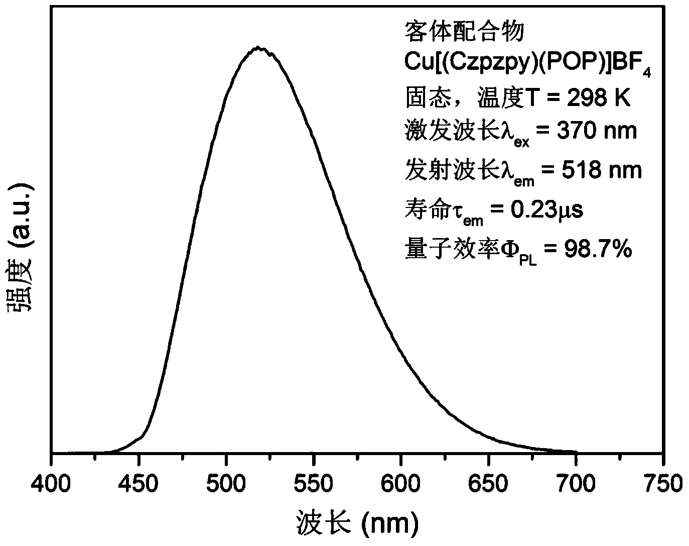
[0092] Preparation: Under nitrogen atmosphere, [Cu(CH 3 EN) 4 ] BF 4 (0.314g, 1mmol) and bis(2-diphenylphosphinophenyl) ether (POP, 0.538g, 1mmol) were added to 10mL of dichloromethane, and after stirring at room temperature for half an hour, the ligand Czpzpy (0.145g, 1mmol ) was added to the solution and stirring was continued for 1 hour. After filtering, the solvent was spin-dried and recrystallized with dichloromethane / ether to obtain light yellow transparent crystals. Utilize nuclear magnetic resonance spectrometer and elemental analyzer to analyze gained complex, the result is as follows:

[0093] 1 H NMR (400MHz, CDCl 3 ):δ8.94(s,1H),8.44(s,1H),8.28(s,1H),8.09(d,J=7.9Hz,2H),7.67–7.27(m,9H),7.25–6.97( m, 11H), 6.91(t, J=7.5Hz, 3H), 6.71–6.18(m, 14H). 31 P NMR: -11.99 (s). Anal. Calcd for C 56 h 42 BCuF 4 N 4 OP 2 : C, 67.31; H, 4.24; N, 5.61. Found: C, 67.04; H, 4.24; N, 5.54.

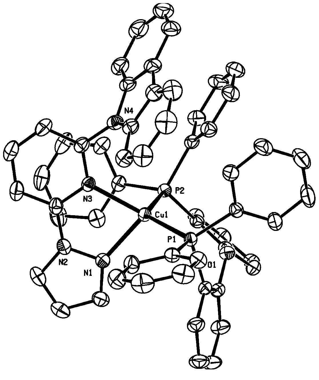
[0094] Crystal struc...

Embodiment 3

[0097] Utilize the host material described in Example 1 and the mixture of the guest complex described in Example 2 to spin-coat the OLED device (device A) that prepares light-emitting layer

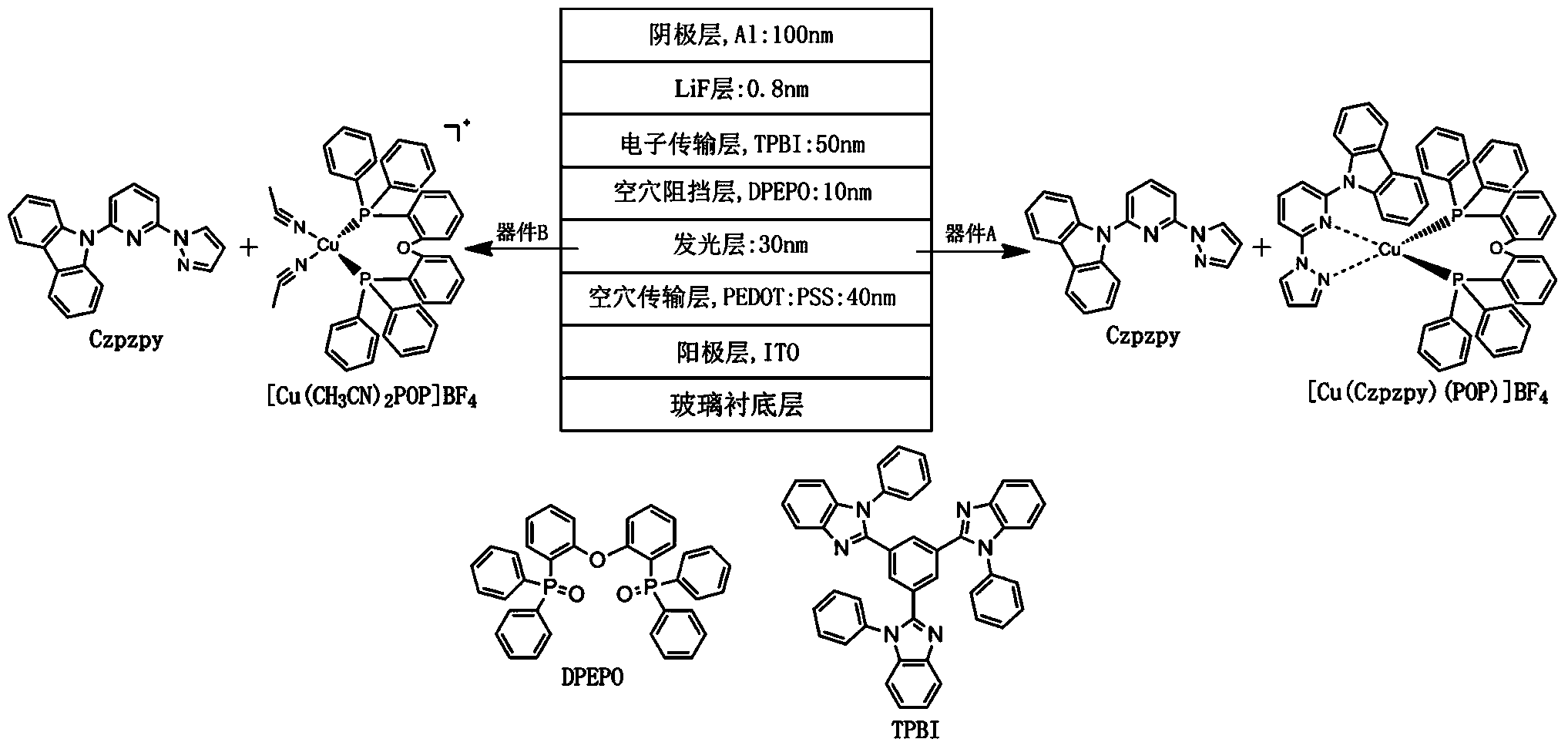
[0098] The preparation method of OLED device A is as follows: spin-coat a layer of PEDOT:PSS (spin for 1 minute, thickness is 40nm) on the clean ITO glass surface under the condition of rotation speed of 3000 rpm, and then dry at 140°C for 20 minutes. 2mg of the guest complex [Cu(Czpzpy)(POP)]BF 4 and 8 mg of Czpzpy were dissolved in 1.8 mL of dichloromethane, and the mixture was spin-coated on the surface of a glass electrode modified by PEDOT:PSS under the condition of a rotating speed of 1500 rpm (rotating for 1 minute) and dried under high vacuum for 1 Hours later, a hole blocking layer (DPEPO) of 10 nm, an electron transport layer (TPBI) of 50 nm, a LiF layer of 0.8 nm and a metal aluminum layer of 100 nm were evaporated sequentially. Device performance is listed in Table 1.


PUM


Abstract

The invention relates to an organic electroluminescent device light-emitting layer and a manufacturing method of the organic electroluminescent device light-emitting layer. The light-emitting layer is a doped system, and main materials of the light-emitting layer can also serve as ligands for forming object coordination compound. The light-emitting layer is manufactured in a solution processing (wet method) technique, so that the light-emitting layer is simple in process and low in cost. When the light-emitting layer is manufactured, the main materials and the object coordination compound are doped, or the main materials are directly doped with initial raw materials for forming the object coordination compound. The initial raw materials react with the main materials in a solution processing process to form the object light-emitting coordination compound to be doped with the residual main materials. The light-emitting layer and the manufacturing method of the light-emitting layer can be applied to organic electroluminescent devices of organic electroluminescent light-emitting diodes (OLEDs) and light-emitting electric chemical cells (LEC).

Description

technical field [0001] The invention relates to a light-emitting layer of an organic electroluminescence device, a preparation method and application thereof, and belongs to the field of organic electroluminescence. Background technique [0002] Organic electroluminescent technology has attracted much attention due to its great potential in the fields of display and lighting. In particular, phosphorescent complexes, as organic electroluminescent materials, break through the limit of 25% exciton utilization efficiency of traditional fluorescent materials, and theoretically the maximum internal quantum efficiency of the device can reach 100%. However, due to the long luminescence lifetime of phosphorescent materials, concentration quenching tends to occur in the luminescent layer, which affects device efficiency. The introduction of the doping system solved this problem well. The doping system is to dope the guest material (ie, phosphorescent dye) into the host material as t...

Claims


Application Information

Patent Timeline
Patent Type & Authority Applications(China)
IPC IPC(8): H01L51/50H01L51/54H01L51/56C07D401/14C07D401/12C07F1/08
CPCC07D401/14C07F1/08H10K71/12H10K85/30H10K85/6572
Inventor 卢灿忠陈旭林
Owner 厦门奥德生物科技有限公司
Learn More