LED epitaxial wafer diffused through Mg, growing method and LED structure

A technology of LED epitaxial wafer and growth method, applied in electrical components, circuits, semiconductor devices, etc., can solve the problems of low luminous efficiency, low hole concentration, low activation efficiency, etc., and achieve increased ionization rate, ionization rate improvement, probability reduced effect

Active Publication Date: 2014-10-08
XIANGNENG HUALEI OPTOELECTRONICS
View PDF6 Cites 15 Cited by
  • Summary
  • Abstract
  • Description
  • Claims
  • Application Information

AI Technical Summary

Problems solved by technology

The significant disadvantage of this prior art is that the p-type gallium nitride layer generally has a constant doping amount of Mg, the activation e

Method used


Image

  • LED epitaxial wafer diffused through Mg, growing method and LED structure
  • LED epitaxial wafer diffused through Mg, growing method and LED structure
  • LED epitaxial wafer diffused through Mg, growing method and LED structure

Examples


Embodiment 1

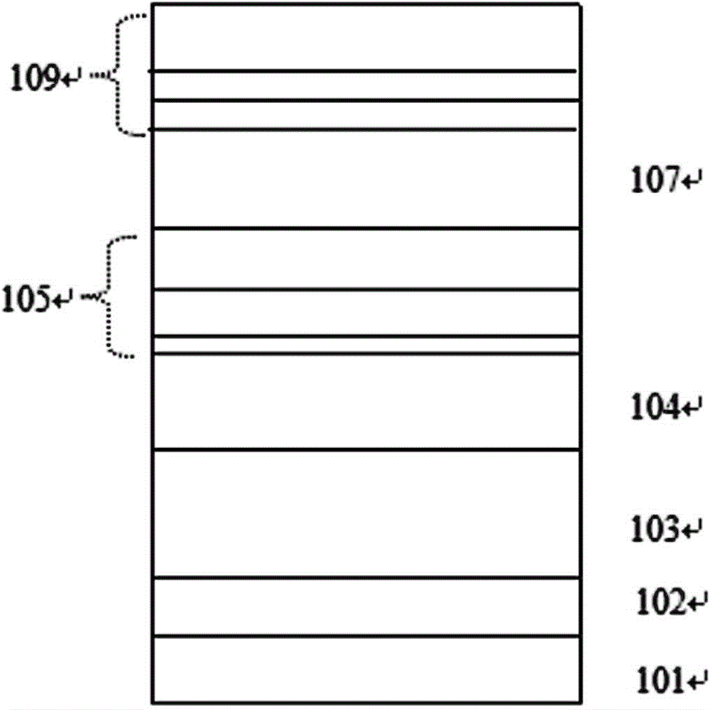
[0033]The present invention adopts Metal Organic Chemical Vapor Deposition (MOCVD, Metalorganic Chemical Vapor Deposition) growth, preferably, the sapphire of (0001) crystal orientation is selected as the substrate, high-purity H 2 or high purity N 2 or high purity H 2 and high purity N 2 The mixed gas is used as the carrier gas, and the metal-organic source and the nitrogen source are trimethylgallium (TMGa), trimethylindium (TMIn), triethylgallium (TEGa), trimethylaluminum (TMAl) and ammonia ( NH 3 ), the n-type dopant is silane (SiH 4 ), the p-type dopant is magnesium dicene (Cp 2 Mg).

[0034] The method for growing Mg-diffused LED epitaxial wafers involves the following growth steps in sequence:

[0035] a. Treat the sapphire substrate at 1000-1200°C for 5-10 minutes under a hydrogen atmosphere with the reaction chamber pressure maintained at 75-150 mbar;

[0036] b. Lower the temperature to 550-650°C, maintain the pressure in the reaction chamber at 400-600mbar, a...

Embodiment 2

[0049] The growth method of Mg-diffused LED epitaxial wafers, the following growth steps are performed in sequence:

[0050] a. Treat the sapphire substrate at 1000-1200°C for 5-10 minutes under a hydrogen atmosphere with the reaction chamber pressure maintained at 150mbar;

[0051] b. Lower the temperature to 550-650°C, maintain the pressure in the reaction chamber at 430mbar, and grow a low-temperature GaN buffer layer with a thickness of 50nm on the sapphire substrate;

[0052] c. Raise the temperature to 1100°C, maintain the pressure in the reaction chamber at 150-300mbar, and continue to grow a non-doped GaN layer with a thickness of 2.8μm;

[0053] d. growing an n-type GaN layer with a thickness of 3.9 μm;

[0054] e. The pressure of the reaction chamber is maintained at 379mbar, and the temperature is lowered to 700°C to grow In-doped In with a thickness of 3.1nm. x Ga (1-x) N layer, the temperature is raised to 850°C to grow a GaN layer with a thickness of 14.3nm, I...

Embodiment 3

[0064] The growth method of Mg-diffused LED epitaxial wafers, the following growth steps are performed in sequence:

[0065] a. Treat the sapphire substrate at 1000-1200°C for 5-10 minutes under a hydrogen atmosphere with the reaction chamber pressure maintained at 86mbar;

[0066] b. Lower the temperature to 550-650°C, maintain the pressure of the reaction chamber at 600mbar, and grow a low-temperature GaN buffer layer with a thickness of 38nm on the sapphire substrate;

[0067] c. Raise the temperature to 1100°C, maintain the pressure of the reaction chamber at 250mbar, and continue to grow a non-doped GaN layer with a thickness of 2.5μm;

[0068] d. growing an n-type GaN layer with a thickness of 2 μm;

[0069] e. The pressure of the reaction chamber is maintained at 400mbar, and the temperature is lowered to 700-750°C to grow In-doped In with a thickness of 3nm. x Ga (1-x) N layer, the temperature is raised to 800-850°C to grow a GaN layer with a thickness of 13nm, In ...


PUM

PropertyMeasurementUnit
Thicknessaaaaaaaaaa
Thicknessaaaaaaaaaa
Thicknessaaaaaaaaaa

Abstract

The invention discloses an LED epitaxial wafer diffused through Mg, a growing method and an LED structure. The LED epitaxial wafer structurally comprises a substrate, a GaN buffering layer, an undoped GaN layer, an n-type GaN layer, a multi-quantum well layer and a P-type AlGaN layer in sequence from bottom to top. A P-type GaN layer doped with Mg in a gradually-changing mode is arranged on the P-type AlGaN layer and is a GaN layer processed through Mg diffusion. The invention further provides the LED structure. The LED epitaxial wafer has the advantages that P-type GaN doped with the Mg in the gradually-changing mode stops growing after growing out a small section, a great deal of the Mg is introduced for carrying out Mg diffusion processing on the front section of the P-type GaN, the Ga position is better replaced by the Mg through the diffusion mode, Mg-H keys are reduced, Mg atoms of filling types are reduced, and therefore most merged Mg atoms are located at the Ga position; moreover, the proportion of the Mg atoms located at the Ga position is increased, and the proportion of the Mg atoms low in ionization energy is increased.

Description

technical field [0001] The invention belongs to the technical field of semiconductors, and relates to a Mg-diffused LED epitaxial wafer, a growth method and an LED structure. Background technique [0002] Gallium nitride-based materials, including InGaN, GaN, and AlGaN alloys, are direct bandgap semiconductors, and the bandgap is continuously adjustable from 1.8-6.2eV. They have excellent properties such as wide direct bandgap, strong chemical bonds, high temperature resistance, and corrosion resistance. It is an ideal material for the production of short-wavelength high-brightness light-emitting devices, ultraviolet light detectors and high-temperature and high-frequency microelectronic devices. It is widely used in full-color large-screen displays, LCD backlights, signal lights, lighting and other fields. [0003] The patent document with the publication number CN102194939A discloses a gallium nitride-based LED epitaxial wafer and its growth method. Its structure includes:...

Claims


Application Information

Patent Timeline
IPC IPC(8): H01L33/14H01L33/04H01L33/00
CPCH01L33/007H01L33/04H01L33/325
Inventor 林传强
Owner XIANGNENG HUALEI OPTOELECTRONICS
Why Eureka
Try Eureka