Microwave integrated amplifier circuit and manufacturing method thereof

An amplifier circuit, microwave integration technology, applied in the field of microelectronics, can solve problems such as relatively high requirements on type and thickness, increase process complexity and cost, process incompatibility, etc., to reduce design difficulty, reduce process complexity, and improve stability. sexual effect

Active Publication Date: 2014-10-22
DYNAX SEMICON
View PDF5 Cites 5 Cited by
  • Summary
  • Abstract
  • Description
  • Claims
  • Application Information

AI Technical Summary

Problems solved by technology

However, the method is still immature, and there are still some problems. First, the doping method generally adopts the ion implantation method, and the process is relatively complicated. In addition to optimizing the implantation conditions, high-temperature annealing is also required to activate the dopant. The process of GaN high electron mobility transistor is not compatible, and its performance may be seriously reduced; secondly, the thin film deposition method requires special sputtering equipment and special sputtering materials, such as TaN, NiCr or other alloy materials, and The process of gallium nitride high electron mobility transistors is also incompatible, which increases the process complexity and cost; third, when making thin film capacitors, it is necessary to deposit a layer of insulating dielectric layer first, and then deposit a layer of conductor as the lower electrode, and then Then deposit a layer of dielectric, and finally deposit the top electrode. The type and thickness of the dielectric are relatively high, and it is not compatible with the process of gallium nitride high electron mobility transistors. It needs to be fabricated separately, which increases the complexity of the process and cost

Method used


Image

  • Microwave integrated amplifier circuit and manufacturing method thereof
  • Microwave integrated amplifier circuit and manufacturing method thereof
  • Microwave integrated amplifier circuit and manufacturing method thereof

Examples


Embodiment 1

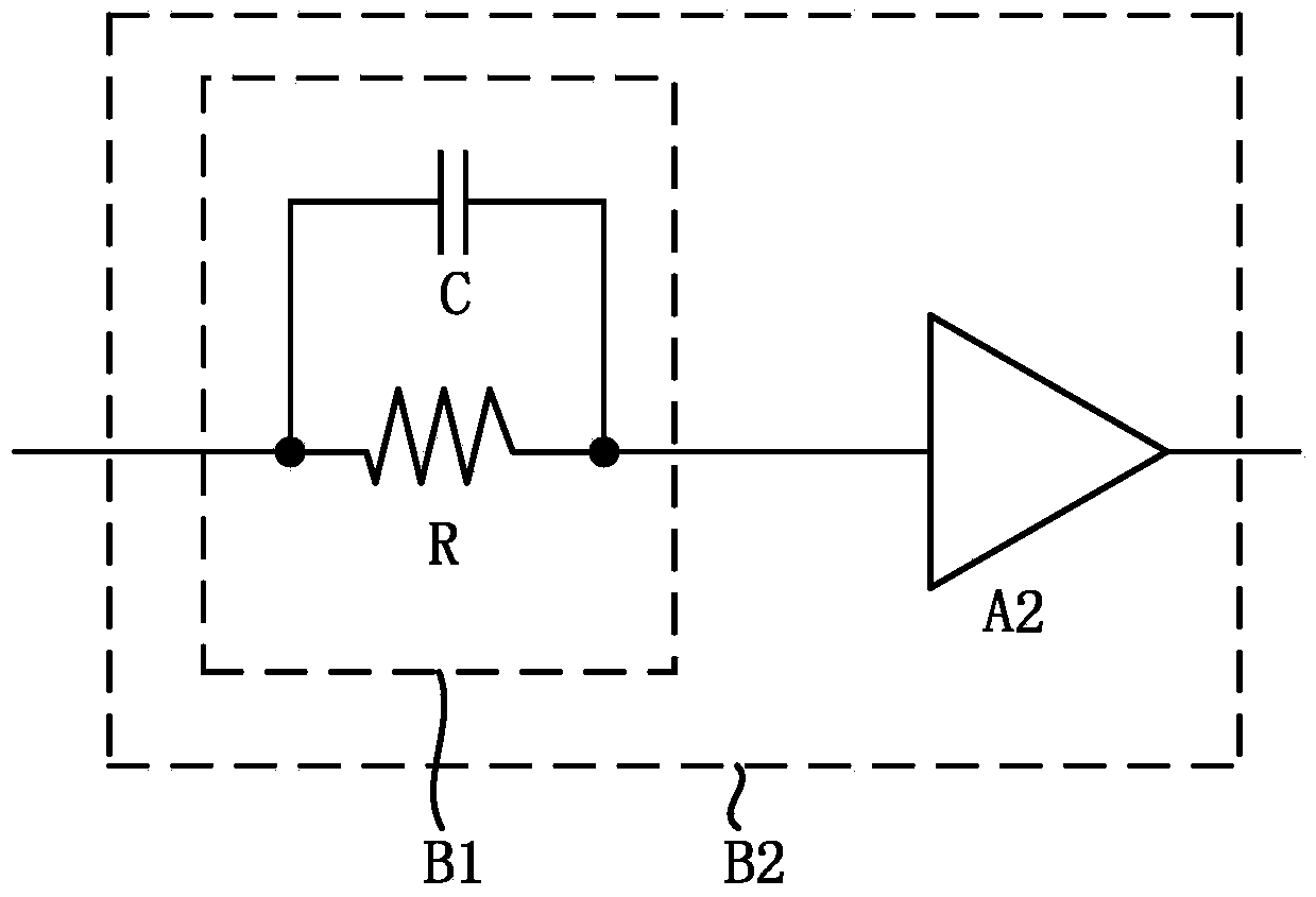
[0070] Embodiment 1 of the present invention provides a microwave integrated amplifier circuit. Figure 2a It is a structural cross-sectional schematic view of a microwave integrated amplifier circuit provided in Embodiment 1 of the present invention. see Figure 2a , the microwave integrated amplifier circuit includes: a gallium nitride high electron mobility transistor 10 and an oscillation stabilization circuit 20, wherein the gallium nitride high electron mobility transistor 10 and the oscillation stabilization circuit 20 have the same substrate 1 and The same epitaxial structure 2 located on the substrate is isolated by the isolation region 31 located in the epitaxial structure 2; the epitaxial structure 2 at least includes a nitride channel layer 2a, located in the nitride channel layer The nitride barrier layer 2b on 2a and the conductive channel 2c with high electron mobility at the interface between the nitride channel layer 2a and the nitride barrier layer 2b; the g...

Embodiment 2

[0082] Embodiment 2 of the present invention also provides a microwave integrated amplifier circuit. Figure 5a It is a structural cross-sectional schematic diagram of a microwave integrated amplifier circuit provided in Embodiment 2 of the present invention. see Figure 5a ,and Figure 2a The difference is that the oscillation stabilization circuit 20 further includes a first dielectric layer 24 , and the first dielectric layer 24 is located between the nitride barrier layer 2 b and the third electrode 23 . Figure 5a It is just a specific example of this embodiment. Figure 5b It is a structural cross-sectional schematic diagram of another microwave integrated amplifier circuit provided by Embodiment 2 of the present invention. see Figure 5b ,and Figure 5a The difference is that the first dielectric layer 24 covers the nitride barrier layer 2 b between the first electrode 21 and the second electrode 22 .

[0083] Further, see Figure 5a and Figure 5b , the first e...

Embodiment 3

[0088] Embodiment 3 of the present invention also provides a microwave integrated amplifier circuit. Figure 6a It is a structural cross-sectional schematic diagram of a microwave integrated amplifier circuit provided by Embodiment 3 of the present invention. see Figure 2a and Figure 6a , on the basis of the first embodiment of the present invention, the oscillation stabilization circuit 20 in the third embodiment of the present invention further includes: a second dielectric layer 25 and a fourth electrode 26, the second dielectric layer 25 is located on the third electrode 23 and on the epitaxial structure 2 between the first electrode 21 and the second electrode 22 and not covered by the third electrode 23, the fourth electrode 26 is located between the first electrode 21 and the second electrode 22 on the second dielectric layer 25 . The rest of the structure of the microwave integrated amplifier circuit in this embodiment and related descriptions are similar to those...


PUM


Abstract

The invention discloses a microwave integrated amplifier circuit and a manufacturing method thereof. The microwave integrated amplifier circuit comprises a gallium nitride high electron mobility transistor and an oscillation stabilizing circuit connected with the gallium nitride high electron mobility transistor. The gallium nitride high electron mobility transistor and the oscillation stabilizing circuit share the same substrate and the same epitaxy structure on the substrate, and the gallium nitride high electron mobility transistor and the oscillation stabilizing circuit are isolated through an isolating area in the epitaxy structure. The designing and manufacturing of resistors and capacitors in the oscillation stabilizing circuit are compatible with process of the gallium nitride high electron mobility transistor, so that the resistors and the capacitors of the oscillation stabilizing circuit and the gallium nitride high electron mobility transistor can be formed simultaneously. Thus, the manufacturing complexity is reduced, and the cost is saved. In addition, the stability of the amplifier circuit is improved, and an oscillation restraining function is achieved. Furthermore, the size and the cost of the amplifier circuit can be reduced, and the designing difficulty of a follow-up microwave match circuit can be reduced. In addition, the effects of lead inductance can be avoided, and the performance of the gain of the amplifier can be improved.

Description

technical field [0001] The invention relates to the technical field of microelectronics, in particular to a microwave integrated amplifier circuit and a manufacturing method thereof. Background technique [0002] Microwave amplifiers employing transistor devices may be referred to as transistor amplifiers. Among transistor devices, the high electron mobility transistor (HEMT) based on gallium nitride (GaN) material has high electron saturation drift speed and breakdown field strength due to the large band gap of gallium nitride material. It has the characteristics of high temperature, good thermal conductivity, etc. It has obvious advantages in the application of high temperature, high frequency, high voltage and high power. It has broad application prospects in the fields of wireless communication and radar system applications. It has become a new research and application hotspot in recent years. [0003] Figure 1a is a schematic circuit diagram of a prior art transistor ...

Claims


Application Information

Patent Timeline
Patent Type & Authority Applications(China)
IPC IPC(8): H03F1/30H01L27/02H01L21/82
Inventor 张乃千
Owner DYNAX SEMICON
Why Eureka
Try Eureka