Graphene/gallium arsenide solar cell and manufacturing method thereof

A technology of solar cells and graphene, applied in the field of solar energy, can solve the problems of complex preparation process of gallium arsenide solar cells, difficulty in wide-scale promotion, high cost, etc., achieve high open circuit voltage and conversion efficiency, and be conducive to industrial application , low cost effect

Inactive Publication Date: 2014-12-24
ZHEJIANG UNIV
View PDF3 Cites 12 Cited by
  • Summary
  • Abstract
  • Description
  • Claims
  • Application Information

AI Technical Summary

Problems solved by technology

However, the traditional gallium arsenide solar cell preparation process is com

Method used


Image

  • Graphene/gallium arsenide solar cell and manufacturing method thereof
  • Graphene/gallium arsenide solar cell and manufacturing method thereof

Examples


Embodiment 1

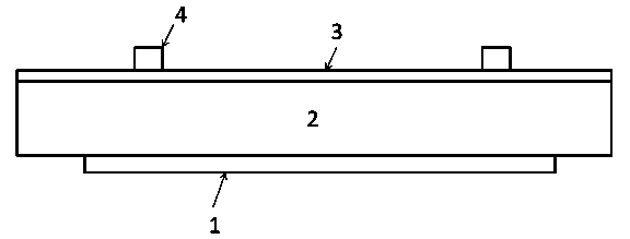
[0021] 1) Deposit a gold electrode on one side of the n-type doped gallium arsenide sheet by electron beam evaporation; then immerse it in 10% NaOH aqueous solution for 1 minute to clean the surface, then take it out and dry it;

[0022] 2) transfer single-layer graphene to the other side of the surface-cleaned gallium arsenide wafer;

[0023] 3) Deposit silver electrodes on graphene by thermal evaporation process to obtain graphene / gallium arsenide solar cells.

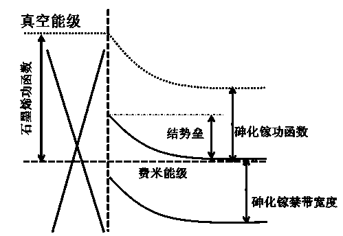
[0024] The basic principle of the resulting graphene / GaAs solar cell is based on the Schottky junction formed by graphene and GaAs, formed by figure 2 The graphene / n-type doped gallium arsenide solar cell energy band schematic diagram shown shows that gallium arsenide has a suitable band gap to convert solar energy into electrical energy, and the work function of graphene is greater than that of n-type doped gallium arsenide The work function of the two materials will form a Schottky junction when they are in conta...

Embodiment 2

[0026] 1) Deposit a palladium electrode on one side of the p-type doped gallium arsenide sheet by magnetron sputtering; then immerse in 20% HCl aqueous solution for 15 minutes to clean the surface, and then take it out and dry it;

[0027] 2) Transfer 10 layers of graphene to the other side of the surface-cleaned GaAs wafer;

[0028] 4) Deposit nickel electrodes on graphene by thermal evaporation process to obtain graphene / gallium arsenide solar cells.

Embodiment 3

[0030] 1) Deposit a chromium / titanium electrode on one side of an n-type doped gallium arsenide wafer using a pulsed laser; then immerse it in HNO with a mass concentration of 10% 3 Clean the surface in the aqueous solution for 30 minutes, then take it out and blow dry;

[0031] 2) Transfer 2 layers of graphene to the other side of the surface-cleaned GaAs wafer;

[0032] 3) Screen-print silver electrodes on graphene to obtain graphene / gallium arsenide solar cells.


PUM


Abstract

The invention relates to a graphene/gallium arsenide solar cell and a manufacturing method thereof. The graphene/gallium arsenide solar cell comprises a back face electrode, an n-type doped or p-type doped gallium arsenide layer, a graphene layer and front face electrodes from top to bottom in sequence, wherein one to 10 layers of graphene is arranged. The manufacturing method comprises the steps that firstly, the back face electrode is manufactured on one face of a gallium arsenide piece; secondly, surface chemical cleaning and drying are conducted; thirdly, the graphene is transferred to the other face of the gallium arsenide piece; fourthly, the front face electrodes are manufactured on the graphene. According to the graphene/gallium arsenide solar cell, the high carrier mobility, the high light transmission and the high conductivity of graphene materials are used, the excellent semiconductor property of gallium arsenide is combined, and thus the solar cell high in conversion efficiency can be easily manufactured on the basis of low cost and the simple technology.

Description

technical field [0001] The invention relates to a solar cell and a manufacturing method thereof, in particular to a graphene / gallium arsenide solar cell and a manufacturing method thereof, belonging to the technical field of solar energy. Background technique [0002] In recent years, solar cells, as a new type of green energy, are playing an increasingly important role in the sustainable development of human beings. Among them, silicon-based solar cells, especially crystalline silicon solar cells, account for ~90% of the market. However, compared with conventional power generation, the cost of solar cell power generation is still high, which limits the large-area application. One of the reasons for the high cost of solar cell power generation is the high cost of cell manufacturing, and another major reason is its low photoelectric conversion efficiency. [0003] Since graphene materials were first stably prepared in 2004, more and more studies have found that graphene mat...

Claims


Application Information

Patent Timeline
IPC IPC(8): H01L31/0352H01L31/07H01L31/18
CPCH01L31/035272H01L31/0725H01L31/18Y02E10/50Y02P70/50
Inventor 林时胜李晓强
Owner ZHEJIANG UNIV
Why Eureka
Try Eureka