

GaN-based heterojunction schottky diode device and preparing method thereof
A Schottky diode and heterojunction technology, which is applied in semiconductor/solid-state device manufacturing, semiconductor devices, electrical components, etc., can solve the problems of single process technology, decline, and complicated operation process, and achieve simple process and good repeatability , the effect of large conduction current
- Summary
- Abstract
- Description
- Claims
- Application Information
AI Technical Summary
Problems solved by technology
Method used
Image

Examples
Embodiment 1
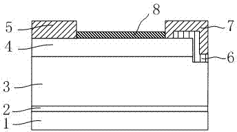
[0053] The fabrication method of the above-mentioned GaN-based heterojunction Schottky diode device is as follows: Figure 4A -F shows, including the following steps:
[0054] ① Using metal-organic chemical vapor deposition (MOCVD) or molecular beam epitaxy (MBE), sequentially grow stress buffer layer 2, high-resistance GaN layer 3 and heterostructure barrier on Si substrate or SiC substrate or sapphire substrate 1 layer 4; as Figure 4A shown;
[0055] ② After the device isolation is completed, dry etching is used to etch the groove 11 in the anode region on the surface of the GaN layer 3 and the heterostructure barrier layer 4, revealing that the groove 11 is composed of the surface of the groove and the surface of the heterostructure barrier layer. the contact surface; such as Figure 4B shown;
[0056] ③Use photolithography technology to open a window at the ohmic contact area of the cathode area, and then vapor-deposit the ohmic contact metal layer 5; Figure 4C sh...
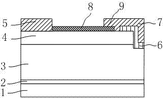
Embodiment 2
[0063] Example 3
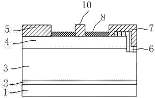
Embodiment 3
PUM
| Property | Measurement | Unit |
|---|---|---|
| depth | aaaaa | aaaaa |
| thickness | aaaaa | aaaaa |
Abstract
Description
Claims
Application Information