Optical fiber F-P strain gauge based on MEMS technology and formation method thereof

An F-P and strain gauge technology, which is applied in the process of producing decorative surface effects, metal material coating process, photo-engraving process of pattern surface, etc. In order to avoid interference spectrum degradation, ensure batch consistency, and wide operating temperature range

Active Publication Date: 2015-04-08
SHANGHAI BAIANTEK SENSING TECH CO LTD
View PDF3 Cites 10 Cited by
  • Summary
  • Abstract
  • Description
  • Claims
  • Application Information

AI Technical Summary

Problems solved by technology

However, these F-P optical interference cavities based on fiber end processing or fiber body micromachining cannot obtain a high-gloss reflective surface, and it is difficult to improve the optical reflectivity of the reflective surface through optical coatings. Therefore, it is difficult to improve the F-P optical interference cavity. The fineness of the interference spectrum makes it difficult to further improve the measurement resolution, and cannot meet the requirements of small-range, high-sensitivity strain measurement applications (such as high-speed wind tunnel aerodynamic measurement, multi-component dynamic force and moment measurement in the industrial field); and because the F-P optical interference cavity The interference fineness factor is low, and only intensity modulation and demodulation and phase modulation and demodulation signal demodulation methods can be used, which are easily affected by light source power fluctuations and fiber bending

Method used


Image

  • Optical fiber F-P strain gauge based on MEMS technology and formation method thereof
  • Optical fiber F-P strain gauge based on MEMS technology and formation method thereof
  • Optical fiber F-P strain gauge based on MEMS technology and formation method thereof

Examples


Embodiment

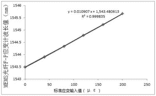
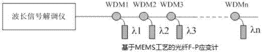
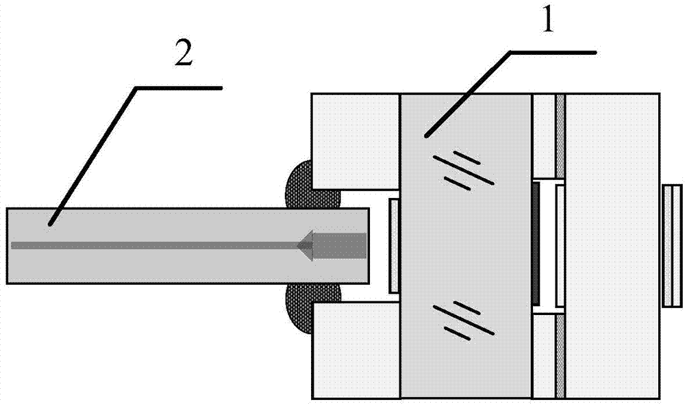
[0054] A structural schematic diagram of an optical fiber F-P strain gauge based on MEMS technology is shown in figure 1 As shown, the optical fiber F-P strain gauge mainly includes a F-P strain-sensitive MEMS chip 1 and a collimated beam expanding optical fiber 2;

[0055] Wherein, the structure schematic diagram of F-P strain-sensitive MEMS chip 1 is shown in Figure 2, and described F-P strain-sensitive MEMS chip 1 is made up of SOI strain beam, glass fixed pole 3 and silicon casing 4;

[0056] The SOI strain beam includes a top layer of silicon 5, an intermediate oxide layer 6, and a bottom layer of silicon 7; wherein, a patterned anti-reflection film 8 and a passivation layer 10 are deposited on one side of the bottom layer of silicon 7, and a highly reflective coating is deposited on the other side. Membrane 9; both the middle oxide layer 6 and the top layer of silicon 5 are processed with central holes, the central holes are coaxial and have the same diameter;

[0057] ...


PUM

PropertyMeasurementUnit
diameteraaaaaaaaaa
reflectanceaaaaaaaaaa

Abstract

The invention discloses an optical fiber F-P strain gauge based on an MEMS technology and a formation method thereof, and belongs to the field of high-precision optical fiber sensing measurement. The optical fiber F-P strain gauge mainly comprises an F-P strain sensitive MEMS chip and a collimated and beam expanded optical fiber. The F-P strain sensitive MEMS chip is composed of an SOI strain beam, a glass fixed pole and a silicon bushing. The SOI strain beam comprises top layer silicon, an intermediate oxide layer and bottom layer silicon. The SOI strain beam is fixed on the glass fixed pole via silicon-glass anodic bonding. The glass fixed pole is fixed on the silicon bushing via silicon-glass anodic bonding. The collimated and beam expanded optical fiber is fixed on the silicon bushing via soldering material. The F-P pressure sensitive MEMS chip is prepared on the basis of an MEMS micromachining technology so that miniaturized and mass manufacturing of the device can be realized. The strain gauge has high-fineness F-P interference spectrum, high sensitivity and high measurement precision can be acquired by adopting wavelength signal demodulation, and series connection of multiple strain gauges on the single-core optical fiber can be realized via wavelength division multiplexing and time division multiplexing.

Description

technical field [0001] The invention relates to an optical fiber F-P strain gauge and a molding method based on MEMS technology, belonging to the field of high-precision optical fiber sensing and measurement. Background technique [0002] In engineering measurement technology, strain measurement is one of the most basic and important technologies. The resistance strain measurement method is a basic traditional means of obtaining strain test data. However, resistance strain gauges have poor fatigue resistance, serious zero drift, and are easily affected by environmental factors such as electromagnetic fields, temperature, humidity, and chemical corrosion, and cannot be used for long-term On-line measurement cannot meet the demand for accurate strain measurement in high temperature and electromagnetic environments. [0003] In recent years, as a new type of measurement method, optical fiber sensor has strong anti-interference (such as electromagnetic field, humidity, chemical...

Claims


Application Information

Patent Timeline
Patent Type & Authority Applications(China)
IPC IPC(8): G01B11/16B81B7/00B81C1/00B81C3/00
Inventor 钟少龙
Owner SHANGHAI BAIANTEK SENSING TECH CO LTD
Why Eureka
Try Eureka