Organic light emitting diode device and preparation method thereof

An electroluminescence device and luminescence technology, which is applied in the direction of electric solid-state devices, semiconductor/solid-state device manufacturing, electrical components, etc., can solve problems such as large light loss, achieve low work function, increase electron tunneling, and reduce light output. Effect

Inactive Publication Date: 2015-04-15
OCEANS KING LIGHTING SCI&TECH CO LTD +2
View PDF0 Cites 7 Cited by
  • Summary
  • Abstract
  • Description
  • Claims
  • Application Information

AI Technical Summary

Problems solved by technology

However, in some practical applications, organic electroluminescent devices need to be transparent when they are not powered on, and it is not necessary to efficiently emit light from both sides when they are powered on. It is only necessary to

Method used


Image

  • Organic light emitting diode device and preparation method thereof
  • Organic light emitting diode device and preparation method thereof
  • Organic light emitting diode device and preparation method thereof

Examples


Embodiment 1

[0055] A method for preparing an organic electroluminescent device, comprising the following steps:

[0056] (1) Clean the transparent ITO glass substrate sequentially with detergent, deionized water, acetone, and ethanol, all of which are cleaned with an ultrasonic cleaner. Each wash is 5 minutes, repeated 3 times, and then dried in an oven. dry; and carry out surface activation treatment to the cleaned ITO glass to increase the oxygen content on the ITO surface and improve the work function of the ITO surface; the ITO thickness is 150nm;

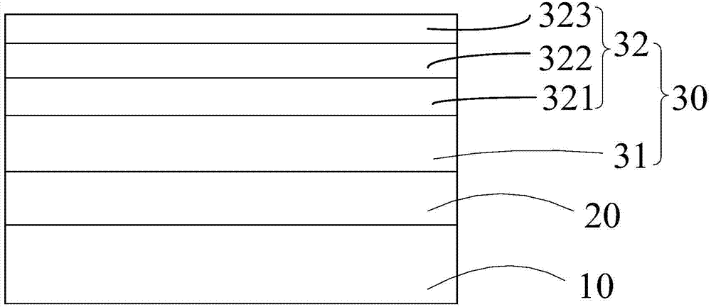
[0057] (2) Prepare a light-emitting functional layer on the surface of the ITO glass substrate by vacuum thermal resistance evaporation, which includes a hole injection layer, a hole transport layer, a light-emitting layer, an electron transport layer, and an electron injection layer in sequence; specifically:

[0058] Preparation of the hole injection layer: the MoO 3 Doped into N,N'-diphenyl-N,N'-di(1-naphthyl)-1,1'-biphenyl-4,4'-diamin...

Embodiment 2

[0071] A method for preparing an organic electroluminescent device, comprising the following steps:

[0072] (1) Clean the transparent ITO glass substrate sequentially with detergent, deionized water, acetone, and ethanol, all of which are cleaned with an ultrasonic cleaner. Each wash is 5 minutes, repeated 3 times, and then dried in an oven. dry; and carry out surface activation treatment to the cleaned ITO glass to increase the oxygen content on the ITO surface and improve the work function of the ITO surface; the ITO thickness is 120nm;

[0073] (2) Prepare a light-emitting functional layer on the surface of the ITO glass substrate by vacuum thermal resistance evaporation, which includes a hole injection layer, a hole transport layer, a light-emitting layer, an electron transport layer, and an electron injection layer in sequence; specifically:

[0074] Preparation of the hole injection layer: the WO 3 Doped into 4,4’,4’’-tris(carbazol-9-yl)triphenylamine (TCTA) as hole in...

Embodiment 3

[0085] A method for preparing an organic electroluminescent device, comprising the following steps:

[0086] (1) Clean the transparent ITO glass substrate sequentially with detergent, deionized water, acetone, and ethanol, all of which are cleaned with an ultrasonic cleaner. Each wash is 5 minutes, repeated 3 times, and then dried in an oven. dry; and carry out surface activation treatment to the ITO glass after cleaning, to increase the oxygen content on the ITO surface, improve the work function of the ITO surface; ITO thickness 100nm;

[0087] (2) Prepare a light-emitting functional layer on the surface of the ITO glass substrate by vacuum thermal resistance evaporation, which includes a hole injection layer, a hole transport layer, a light-emitting layer, an electron transport layer, and an electron injection layer in sequence; specifically:

[0088] Preparation of the hole injection layer: the V 2 o 5 Doped into 4,4’-bis(9-carbazole)biphenyl (CBP) as hole injection laye...


PUM

PropertyMeasurementUnit
Widthaaaaaaaaaa
Thicknessaaaaaaaaaa
Thicknessaaaaaaaaaa

Abstract

The invention provides an organic light emitting diode device. The organic light emitting diode device includes a transparent electric conduction anode substrate as well as a light-emitting functional layer and a cathode which are sequentially stacked on the transparent electric conduction anode substrate, wherein the cathode includes a cathode layer and a second cathode layer which are stacked sequentially; the first cathode layer comprises a plurality of strip-shaped oxide/metal/oxide composite layers which are arranged on the light-emitting functional layer at intervals; the second cathode layer comprises a metal oxide layer, an alloy layer and an electric conduction oxide thin film layer which are stacked sequentially, wherein the metal oxide layer is made of at least two kinds of materials selected from Nb2O5, V2O5 and Ta2O5, and the alloy layer is made of magnesium-silver alloy or lithium-aluminum alloy. The organic light emitting diode device can be adopted as a transparent product when not being lit; and when the organic light emitting diode device works normally, the light extraction contrast of the anode and cathode is (15 to 20):1. The invention also provides a preparation method of the organic light emitting diode device.

Description

technical field [0001] The invention relates to an organic electroluminescent device, in particular to an organic electroluminescent device and a preparation method thereof. Background technique [0002] Organic Light Emission Diode, hereinafter referred to as OLED, has the characteristics of high brightness, wide range of material selection, low driving voltage, fully cured active light emission, etc., and has the advantages of high definition, wide viewing angle, and fast response speed. It is a display technology and light source with great potential, which conforms to the development trend of mobile communication and information display in the information age, as well as the requirements of green lighting technology, and is the focus of many researchers at home and abroad. [0003] Transparent organic electroluminescent device (TOLED) is a kind of OLED. It can emit light on both sides of the anode and cathode when it is powered on, and it becomes transparent when it is n...

Claims


Application Information

Patent Timeline
IPC IPC(8): H01L51/50H01L51/52H01L51/54H01L51/56
CPCH10K50/822H10K50/82H10K71/00
Inventor 周明杰钟铁涛王平张振华
Owner OCEANS KING LIGHTING SCI&TECH CO LTD
Why Eureka
Try Eureka