Organic light emitting diode device and preparation method thereof

An electroluminescence device and electroluminescence technology, which are applied in the direction of electric solid device, semiconductor/solid state device manufacturing, electrical components, etc., to achieve the effect of compact structure, good flatness and strong corrosion resistance.

Inactive Publication Date: 2015-04-15
OCEANS KING LIGHTING SCI&TECH CO LTD +2
View PDF0 Cites 5 Cited by
  • Summary
  • Abstract
  • Description
  • Claims
  • Application Information

AI Technical Summary

Problems solved by technology

The method of the invention is especially suitable for e

Method used


Image

  • Organic light emitting diode device and preparation method thereof

Examples


Embodiment 1

[0055] Such as figure 1 The schematic diagram of the structure of the organic electroluminescent device is shown. This embodiment provides a method for preparing an organic electroluminescent device, which includes the following steps:

[0056] (1) Prepare the light-emitting functional layer 20 and the cathode layer 30 on the anode substrate

[0057] a. Pretreatment of conductive glass substrate

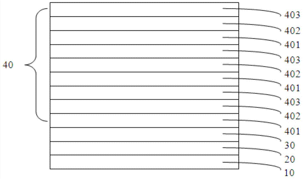
[0058] Take the ITO glass substrate 10, and perform acetone cleaning→ethanol cleaning→deionized water cleaning→ethanol cleaning in sequence, all cleaning with an ultrasonic cleaning machine, washing and cleaning for 5 minutes, then blowing dry with nitrogen, and drying in an oven for later use; The cleaned ITO glass also needs surface activation treatment to increase the oxygen content of the conductive surface layer and improve the work function of the conductive layer surface; the thickness of ITO is 100nm;

[0059] b. Preparation of luminescent functional layer 20 and cathode la...

Embodiment 2

[0078] A method for preparing an organic electroluminescent device, comprising the following steps:

[0079] (1) Preparation of luminescent functional layer and cathode layer on the anode substrate

[0080] With embodiment one;

[0081] (2) Prepare the encapsulation layer on the cathode layer

[0082] a. Fabrication of silicon oxynitride barrier layer:

[0083] A silicon oxynitride barrier layer is deposited on the surface of the cathode layer 30 by plasma enhanced chemical vapor deposition (PECVD). The silicon oxynitride barrier layer is made of silicon oxynitride, and the thickness of the deposited silicon oxynitride barrier layer is In the process of depositing the silicon oxynitride barrier layer 401, the deposition temperature is 50°C, and the gas sources used are hexamethyldisilamine (HMDS), ammonia (NH 3 ), oxygen (O 2 ) and argon (Ar), wherein, the HMDS, NH 3 , O 2 The flows of Ar and Ar are 14sccm, 18sccm, 18sccm and 80sccm respectively;

[0084] b. Fabrication...

Embodiment 3

[0091] A method for preparing an organic electroluminescent device, comprising the following steps:

[0092] (1) Preparation of luminescent functional layer and cathode layer on the anode substrate

[0093] With embodiment one;

[0094] (2) Prepare the encapsulation layer on the cathode layer

[0095] a. Fabrication of silicon oxynitride barrier layer:

[0096] A silicon oxynitride barrier layer is deposited on the surface of the cathode layer 30 by plasma enhanced chemical vapor deposition (PECVD). The silicon oxynitride barrier layer is made of silicon oxynitride, and the thickness of the deposited silicon oxynitride barrier layer is In the process of depositing the silicon oxynitride barrier layer 401, the deposition temperature is 40°C, and the gas sources used are hexamethyldisilamine (HMDS), ammonia (NH 3 ), oxygen (O 2 ) and argon (Ar), wherein, the HMDS, NH 3 , O 2 The flows of Ar and Ar are 12sccm, 15sccm, 16sccm and 76sccm respectively;

[0097] b. Fabrication...


PUM

PropertyMeasurementUnit
Thicknessaaaaaaaaaa
Thicknessaaaaaaaaaa
Thicknessaaaaaaaaaa

Abstract

The invention provides an organic light emitting diode device. The organic light emitting diode device include an anode electric conduction substrate, a light-emitting functional layer, a cathode layer and an encapsulation layer which are stacked to one another sequentially; the encapsulation layer comprises at least one encapsulation unit, wherein the encapsulation unit includes a silicon oxynitride barrier layer, a first inorganic barrier layer and a second inorganic barrier layer which are stacked to one another sequentially, wherein the silicon oxynitride barrier layer is made of a silicon oxynitride compound, and the first inorganic barrier layer is made of an oxide of IIIA-family metal, and the second inorganic barrier layer is made of an oxide of IVB-family metal. According to the organic light emitting diode device, multi-layer material alternate encapsulation is adopted, so that the organic light emitting diode device has high density, and erosion of the organic light emitting diode device, which is caused by oxygen and water vapor, can be effectively reduced, and therefore, the service life of the organic light emitting diode device can be greatly prolonged. The invention also provides a preparation method of the organic light emitting diode device.

Description

technical field [0001] The invention relates to an organic electroluminescent device, in particular to an organic electroluminescent device and a preparation method thereof. Background technique [0002] Organic electroluminescent device (OLED) is a current-mode semiconductor light-emitting device based on organic materials. Its typical structure is that a multi-layer organic material film (hole injection layer, hole transport layer, light emitting layer, electron transport layer and electron injection layer) is sandwiched between the transparent anode and cathode layers. When a certain voltage is applied between the electrodes , the luminescent layer will emit light. In recent years, due to its low production cost, short response time, high luminance, wide viewing angle, low driving voltage, energy saving and environmental protection, organic electroluminescent devices have received extensive attention in the fields of full-color display, backlight and lighting. And it is...

Claims


Application Information

Patent Timeline
IPC IPC(8): H01L51/52H01L51/54H01L51/56
CPCH10K50/8445H10K50/844
Inventor 周明杰钟铁涛王平张振华
Owner OCEANS KING LIGHTING SCI&TECH CO LTD
Why Eureka
Try Eureka