Semi-insulated GaN film and preparation method thereof

A semi-insulating, thin-film technology, used in semiconductor/solid-state device manufacturing, semiconductor devices, electrical components, etc., can solve problems such as reducing the electron migration rate, and achieve the effects of low cost, high purity, and simple operation methods.

Inactive Publication Date: 2015-07-01
江西省昌大光电科技有限公司
View PDF5 Cites 8 Cited by
  • Summary
  • Abstract
  • Description
  • Claims
  • Application Information

AI Technical Summary

Problems solved by technology

However, due to the strong scattering effect of transition metals, it will reduce the mobility of electrons in the channel layer of HEMT devices.

Method used


Image

  • Semi-insulated GaN film and preparation method thereof
  • Semi-insulated GaN film and preparation method thereof

Examples


Embodiment 1

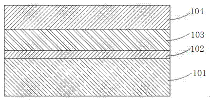
[0025] Such as figure 1 As shown, the present invention provides a method for preparing a semi-insulating GaN thin film, which includes the following steps: first, a sapphire substrate 101 with a (0001) crystal orientation is placed in an MOCVD reaction chamber; 2 In the environment, the temperature is raised to 1180°C for high-temperature treatment of the substrate for 10 minutes; the temperature is lowered to 550°C, and a 25nm thick GaN buffer layer 102 is grown at 600mbar; the temperature is raised to 1150°C to grow a 2um thick non-doped GaN template 103; Under 50torr, carbon tetrachloride doping gas was introduced to grow a carbon concentration of 1×10 18 cm -3 3um thick semi-insulating gallium nitride thin film layer 104; cool down to room temperature, and the growth ends.

Embodiment 2

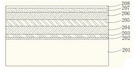
[0027] Such as figure 2 As shown, the structure schematic diagram of the high electron mobility transistor epitaxial material prepared by the present invention. First, put the silicon substrate 201 into the growth chamber of the MOCVD system; then in the H 2 In the environment, the temperature was raised to 1180°C for high-temperature treatment of the substrate for 10 minutes; the temperature was lowered to 1060°C, and trimethylaluminum was passed through for 20 seconds to form an Al layer 202 on the surface of the silicon substrate; ammonia gas and trimethylaluminum were passed through to grow a 100nm AlN layer 203; Ammonia gas, trimethylaluminum and trimethylgallium are introduced to grow a 0.5um thick AlGaN layer 204; Trimethylaluminum is turned off, and the temperature is raised to 1150°C to grow a 1.0um thick non-doped GaN template 205; At 1150°C and 600torr, carbon tetrabromide doping gas was introduced to grow a carbon concentration of 1×10 18 cm -3 2um thick semi-...


PUM

PropertyMeasurementUnit
thicknessaaaaaaaaaa
temperatureaaaaaaaaaa

Abstract

The invention provides a semi-insulated GaN film and a preparation method thereof. The method comprises the steps of preparing a substrate; developing a buffering layer on the substrate by the metal organic chemical vapor deposition method; developing a gallium nitride die plate on the buffering layer; developing a carbon-doped semi-insulated gallium nitride film layer on the gallium nitride die plate. The semi-insulated gallium nitride prepared by the method is high in quality, high in purity, small in impurity memory effect, and high in insulating performance, and can effectively reduce current leakage.

Description

technical field [0001] The invention belongs to the technical field of semiconductors, and in particular relates to a semi-insulating GaN thin film and a preparation method thereof. Background technique [0002] GaN has the characteristics of large direct band gap (3.4ev), high thermal conductivity, and high electron saturation drift velocity, so it has become a research hotspot in the field of semiconductor technology. In particular, GaN-based high electron mobility field-effect transistors (HEMTs) are a new class of electronic devices based on nitride heterostructures. The device has excellent characteristics of high frequency and high power, and is widely used in information transmission and reception, energy conversion and other fields such as wireless communication base stations and power electronic devices. [0003] Due to the high breakdown voltage of AlGaN / GaN heterostructure, high concentration two-dimensional electron gas (2DEG) can be generated due to polarizatio...

Claims


Application Information

Patent Timeline
Patent Type & Authority Applications(China)
IPC IPC(8): H01L21/02H01L29/207H01L21/335
Inventor 陈振
Owner 江西省昌大光电科技有限公司
Why Eureka
Try Eureka