
Method for achieving electronic building brick high-temperature packaging by filling Sn-based solder with micro-nano metallic particles

A technology of metal particles and electronic components, applied in metal processing, metal processing equipment, welding/cutting media/materials, etc., can solve the problems of high cost of nanomaterial preparation, device damage, long preparation time, etc., and achieve heat dissipation and electrical performance The effect of index improvement, high temperature resistance capability enhancement, and service temperature increase

Active Publication Date: 2015-07-08
HARBIN INST OF TECH
View PDF7 Cites 26 Cited by
  • Summary
  • Abstract
  • Description
  • Claims
  • Application Information

AI Technical Summary

Problems solved by technology

According to the thermodynamic properties of nano-silver particles, the connection can be realized under the condition of less than 200°C, and the formation of joints can be used under the condition of more than 350°C, but the connection of nanoparticles takes a long time, the joint is porous structure, and the preparation cost of nano-materials Higher, which restricts the application of such materials; joints formed by all intermetallic compounds can be applied under high temperature conditions, but generally take a long time to prepare, and it is difficult to achieve large-scale industrial applications; intermetallic compound nanoparticle solder paste sintering needs to use The sintering is realized at a specification higher than or close to the melting point of the intermetallic compound, and the melting point of the intermetallic compound is generally higher (over 400°C), which may easily cause damage to the device during the connection process

Method used


Image

  • Method for achieving electronic building brick high-temperature packaging by filling Sn-based solder with micro-nano metallic particles

Examples


Embodiment 1

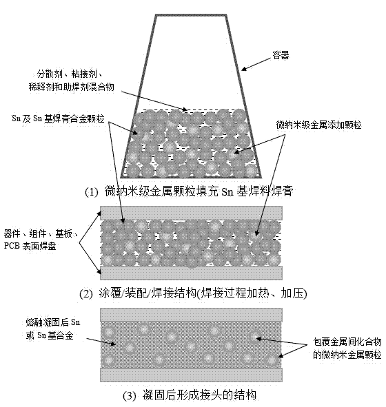
[0018] Such as figure 1 As shown, the micron-scale Cu metal particle filling Sn-based solder solder paste interconnection joint formation method comprises the steps:

[0019] Step 1: preparing Cu particles with a diameter of about 20 μm;

[0020] Step 2: Mix the above micron-sized Cu particles with the dispersant methyl amyl alcohol, the binder α-terpineol, the diluent terpineol, and the flux rosin in an appropriate amount, and the mixing mass ratio is 80:4:6:4: 6;

[0021] Step 3: Mix the above Cu particle mixture with Sn3.5wt.%Ag solder paste, the Cu particle mixture accounts for 50% of the total mass of the final solder paste mixture;

[0022] Step 4: Use 200W ultrasonic vibration for 80 minutes to make the Cu particles uniformly dispersed in the mixture prepared in Step 3 to make a micron-sized metal particle filled Sn-based solder paste;

[0023] Step 5: Place the Sn-based solder paste filled with the above micron-sized metal particles on the substrate by the screen pr...

Embodiment 2

[0026] The nanoscale Ag metal particle filling Sn-based solder paste interconnection joint forming method comprises the following steps:

[0027] Step 1: preparing Ag particles with a diameter of about 100 nm;

[0028] Step 2: mix the above nano-Ag particles with dispersant triethylhexyl phosphoric acid, binder α-terpineol, diluent alcohol, flux rosin in an appropriate amount, and the mixing ratio is 85:3:4:4:4;

[0029] Step 3: Mix the above nanoscale Ag particle mixture with Sn0.7wt.%Cu solder paste, the Ag particle mixture accounts for 30% of the total mass of the final solder paste mixture;

[0030] Step 4: Use 150W ultrasonic vibration for 120 minutes to make the Ag particles uniformly dispersed in the mixture prepared in Step 3 to make nano-scale Ag metal particles filled with Sn-based solder paste;

[0031] Step 5: Fill the above nano-scale Ag metal particles with Sn-based solder paste by dispensing method, complete the alignment of the pads of the parts to be soldered...

Embodiment 3

[0033] Embodiment 3: The method for forming interconnection joints filled with Sn-based solder paste by nano-scale Cu metal particles comprises the following steps:

[0034] Step 1: Prepare Cu particles with a diameter of about 500 nm;

[0035]Step 2: Mix the above micron-sized Cu particles with the dispersant methyl amyl alcohol, the binder α-terpineol, the diluent terpineol, and the flux rosin in an appropriate amount, and the mixing mass ratio is 82:4:5:4: 5;

[0036] Step 3: mixing the above Cu particle mixture with pure Sn solder paste, the Cu particle mixture accounts for 60% of the total mass of the final solder paste mixture;

[0037] Step 4: Use 180W ultrasonic vibration for 100 minutes to make Cu particles uniformly dispersed in the mixture prepared in Step 3 to make nano-scale metal particles filled Sn-based solder paste;

[0038] Step 5: Place the above nanoscale metal particles filled Sn-based solder paste on the substrate by screen printing method, complete the...


PUM

PropertyMeasurementUnit
diameteraaaaaaaaaa
diameteraaaaaaaaaa
melting pointaaaaaaaaaa

Abstract

The invention provides a method for achieving electronic building brick high-temperature packaging by filling Sn-based solder with micro-nano metallic particles. The method comprises the steps that the micro-nano metallic particles are prepared and mixed with a dispersing agent, a caking agent, diluent and scaling powder; a micro-nano metallic particle mixture is evenly mixed with pure Sn or Sn-based soldering paste; the Sn-based soldering paste is filled with the micro-nano metallic particles and placed on a base plate, alignment process of a part to be welded is completed, and pressure is exerted on the Sn-based soldering paste; the Sn-based soldering paste is put back in a reflow oven and experiences a preheating stage, an insulation stage, a reflowing stage and a cooling stage. According to the method for achieving electronic building brick high-temperature packaging by filling the Sn-based solder with the micro-nano metallic particles, the Sn-based solder is filled with the micro-nano metallic particles, connection and assembly of high-power devices or components can be achieved under the process condition of being compatible with traditional reflow soldering, when the devices serve at high temperature, metallic particles are formed inside a connector, excellent conductivity property and heat-conducting property are achieved, and the heat dissipation index and the electrical performance index of the electronic building brick can be significantly improved.

Description

technical field [0001] The invention belongs to the technical field of micro-interconnection of electronic packaging, relates to a method for packaging and interconnecting electronic components and modules, in particular to a method for filling Sn-based solder with micronano-level metal particles to realize high-temperature packaging of electronic components. Background technique [0002] Electronic packaging micro-interconnection technology is one of the core technologies for the packaging of various electronic components, modules, and components. As the electronics industry continues to increase the demand and indicators for high-power and high-density packaging of electronic components, modules, and components, the service temperature of electronic components, modules, and components will also continue to increase, which will pose a challenge to micro-interconnection materials. More stringent requirements, however, traditional solder alloys and resin bonding materials are...

Claims


Application Information

Patent Timeline
Patent Type & Authority Applications(China)
IPC IPC(8): B23K1/008B23K1/20B23K35/26B23K35/363
CPCB23K1/012B23K1/20B23K35/025B23K35/262B23K35/362B23K2101/36
Inventor 刘威郑振王春青
Owner HARBIN INST OF TECH
Learn More