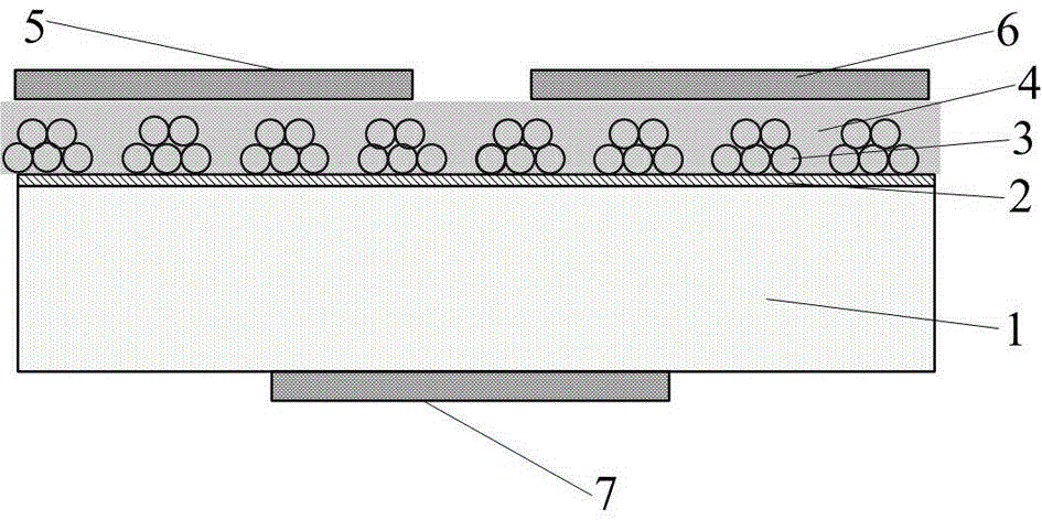
Metal quantum dot/organic semiconductor composite conductive channel film transistor preparation method
A technology of organic semiconductors and thin film transistors, which is applied in the field of preparation of metal quantum dots/organic semiconductor composite conductive channel thin film transistors, can solve the problems of limited overall device performance, sensitivity, limited switching frequency and speed, and difficulties in meeting demands, and achieve Improved sensitivity and output transfer characteristics, flexible and controllable device performance, and novel preparation methods
- Summary
- Abstract
- Description
- Claims
- Application Information
AI Technical Summary
Problems solved by technology
Method used
Image
Examples
Embodiment 1
[0033] (1) Weigh metal ion-containing compounds such as silver nitrate or HAuCl4 in proportion: sodium linoleate: absolute ethanol: linoleic acid = 0.3:1.0:5:0.5, then pour the mixture into the reaction kettle, and Add an appropriate amount of deionized water so that the volume of the mixed liquid accounts for 40% of the total volume of the reactor, stir and mix evenly, heat-treat at 20°C for 30 minutes, and then repeatedly deionized water / absolute ethanol and high-speed centrifugation of the reaction product After cleaning, the final product is dispersed in cyclohexane to obtain the corresponding metal quantum dot solution;
[0034] (2) Take a silicon / silicon dioxide substrate with a size of 1cm×1cm and an oxide layer (silicon dioxide film) thickness of 30nm, figure 1 It is a schematic diagram of the silicon / silicon dioxide substrate structure, where 1 is the substrate silicon, and 2 is the silicon dioxide film on the silicon surface. The silicon / silicon dioxide substrate wa...
Embodiment 2
[0039] (1) Weigh metal ion-containing compounds such as silver nitrate or HAuCl4 in proportion: sodium linoleate: absolute ethanol: linoleic acid = 0.7:1.5:10:1.5, then pour the mixture into the reaction kettle, and Add an appropriate amount of deionized water so that the volume of the mixed solution accounts for 50% of the total volume of the reactor, stir and mix evenly, and heat-treat at 140°C for 200 minutes, then repeatedly deionized water / absolute ethanol and high-speed centrifugation of the reaction product After cleaning, the final product is dispersed in cyclohexane to obtain the corresponding metal quantum dot solution;
[0040] (2) Take a silicon / silicon dioxide substrate with a size of 1cm×1cm and an oxide layer thickness of 200nm, figure 1 It is a schematic diagram of the silicon / silicon dioxide substrate structure, where 1 is the substrate silicon, and 2 is the silicon dioxide film on the silicon surface. The silicon / silicon dioxide substrate was cleaned at high...
Embodiment 3
[0045] (1) Weigh metal ion-containing compounds such as silver nitrate or HAuCl4 in proportion: sodium linoleate: absolute ethanol: linoleic acid=1.0: 2.0: 15: 2.5, then pour the mixture into the reaction kettle, and Add an appropriate amount of deionized water so that the volume of the mixed liquid accounts for 60% of the total volume of the reactor, stir and mix evenly, heat-treat at 200°C for 400 minutes, and then repeatedly deionized water / absolute ethanol and high-speed centrifugation of the reaction product After cleaning, the final product is dispersed in cyclohexane to obtain the corresponding metal quantum dot solution;
[0046] (2) Take a silicon / silicon dioxide substrate with a size of 1cm×1cm and an oxide layer thickness of 300nm, figure 1 It is a schematic diagram of the silicon / silicon dioxide substrate structure, where 1 is the substrate silicon, and 2 is the silicon dioxide film on the silicon surface. The silicon / silicon dioxide substrate was cleaned at high ...
PUM
| Property | Measurement | Unit |
|---|---|---|
| Thickness | aaaaa | aaaaa |
| Thickness | aaaaa | aaaaa |
Abstract
Description
Claims
Application Information
 - Generate Ideas
- Intellectual Property
- Life Sciences
- Materials
- Tech Scout
- Unparalleled Data Quality
- Higher Quality Content
- 60% Fewer Hallucinations
Browse by: Latest US Patents, China's latest patents, Technical Efficacy Thesaurus, Application Domain, Technology Topic, Popular Technical Reports.
© 2025 PatSnap. All rights reserved.Legal|Privacy policy|Modern Slavery Act Transparency Statement|Sitemap|About US| Contact US: help@patsnap.com


