Method for detecting microdefects of quasi monocrystalline silicon sheets

A detection method and micro-defect technology, applied in the direction of sustainable manufacturing/processing, electrical components, climate sustainability, etc., to achieve the effects of convenient operation, optimized manufacturing process, and fast and accurate testing methods

Inactive Publication Date: 2015-09-09
连云港市产品质量监督检验中心
View PDF9 Cites 23 Cited by
  • Summary
  • Abstract
  • Description
  • Claims
  • Application Information

AI Technical Summary

Problems solved by technology

[0007] At present, there is a lack of a fast and accurate test

Method used


Image

  • Method for detecting microdefects of quasi monocrystalline silicon sheets
  • Method for detecting microdefects of quasi monocrystalline silicon sheets
  • Method for detecting microdefects of quasi monocrystalline silicon sheets

Examples


Embodiment 1

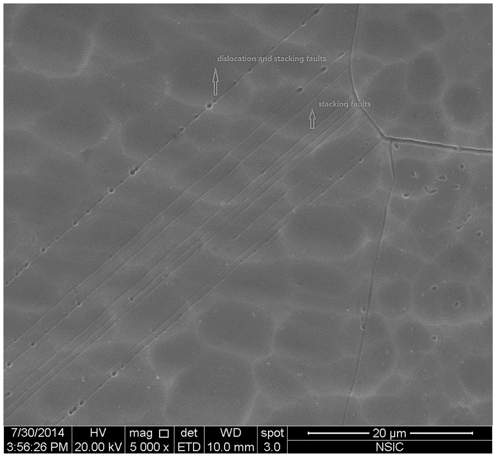
[0037] Taking a cast quasi-single crystal silicon wafer produced by a large-scale photovoltaic crystalline silicon material enterprise as a sample, the invention provides a method for detecting micro-defects in a quasi-single crystal silicon wafer, which includes the following steps:

[0038] (1) Manual mechanical polishing: the quasi-monocrystalline silicon wafer to be etched is manually mechanically polished, and rinsed with deionized water; The thickness of the polishing pad is 2 mm, the polishing solution is a solution of ultrafine silicon carbide water suspension or nano silicon dioxide slurry added with 1% hydrogen peroxide by volume, and the rotating speed of the polishing disc is 30 r / min.

[0039] (2) chemical corrosion polishing: the silicon chip after mechanical polishing is cleaned is carried out chemical corrosion polishing, and rinses with deionized water; A mixed solution of nitric acid and hydrofluoric acid; the content of hydrofluoric acid in said hydrofluoric...

Embodiment 2

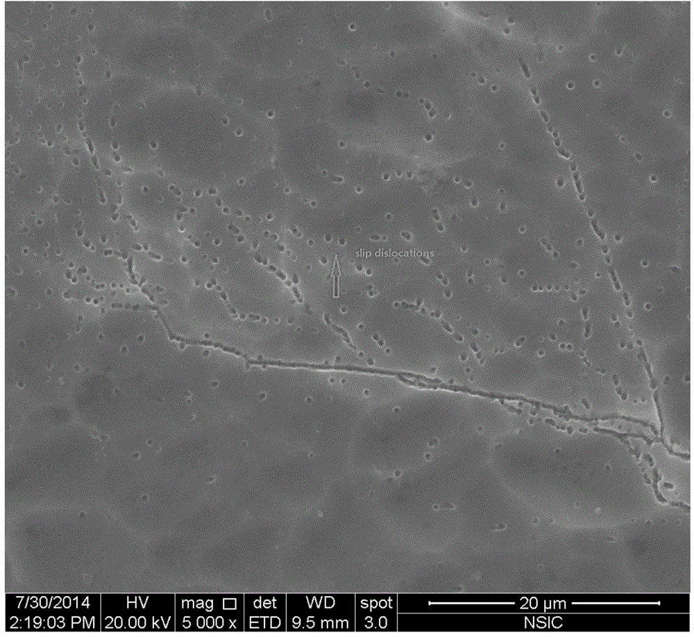
[0061] The difference between embodiment 2 and embodiment 1 is that the present invention provides a method for detecting micro-defects in quasi-single crystal silicon wafers, comprising the following steps:

[0062] In step (1), manual mechanical polishing: perform manual mechanical polishing on the quasi-single crystal silicon wafer to be corroded, and rinse with deionized water; The thickness of the single crystal silicon wafer is 3 mm, the polishing solution is a solution of superfine silicon carbide aqueous suspension or nano silicon dioxide slurry added with 1% hydrogen peroxide by volume, and the rotational speed of the polishing disc is 36 r / min.

[0063] In step (2), chemical etching and polishing: the mechanically polished silicon wafer is chemically etched and polished, and rinsed with deionized water; after the mechanical polishing, the silicon wafer is cleaned and the silicon wafer is chemically etched with an etching solution. Said corrosion solution is nitric ac...

Embodiment 3

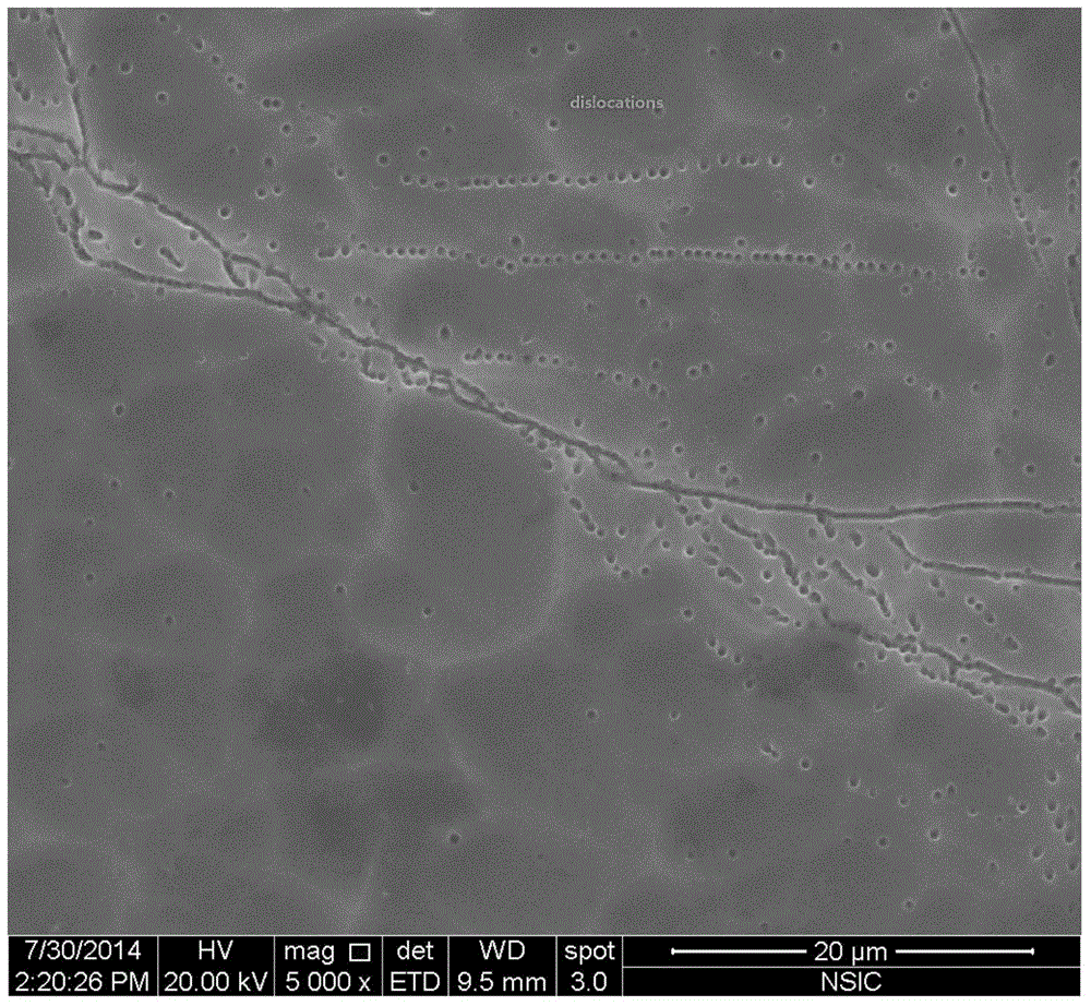
[0066] The difference between embodiment 3 and embodiment 2 is that the present invention provides a method for detecting micro-defects in quasi-single crystal silicon wafers, comprising the following steps:

[0067] In step (1), manual mechanical polishing: perform manual mechanical polishing on the quasi-single crystal silicon wafer to be corroded, and rinse with deionized water; The thickness of the monocrystalline silicon wafer is 3 mm, the polishing solution is a solution of ultrafine silicon carbide water suspension or nano silicon dioxide slurry added with 1% hydrogen peroxide by volume, and the rotational speed of the polishing disc is 40 r / min.

[0068] In step (2), chemical etching and polishing: the mechanically polished and cleaned silicon wafers are chemically etched and polished, and rinsed with deionized water; after mechanical polishing, the silicon wafers are cleaned and chemically etched with an etching solution. Said corrosion solution is nitric acid and hyd...


PUM

PropertyMeasurementUnit
Thicknessaaaaaaaaaa
Thicknessaaaaaaaaaa
Thicknessaaaaaaaaaa

Abstract

The invention discloses a method for detecting microdefects of quasi monocrystalline silicon sheets. The method includes a manually and mechanically polishing step of manually and mechanically polishing aquasi monocrystalline silicon sheet to be etched and flushing the quasi monocrystalline silicon sheet with deionized water; a chemical etch polishing step of chemically etching and polishing the silicon sheet subjected to the mechanical polishing and rinsing the silicon sheet with deionized water; a preferential microdefect etching step of carrying out preferential microdefect etching on the silicon sheet subjected to the chemically etching and polishing, rinsing the silicon sheet with deionized water and drying the silicon sheet in a baking oven; and a microdefect observation process of carrying out minority carrier lifetime and iron-boron opposite scanning for the etched silicon chip, observing the minority carrier lifetime scanning color distribution by a metallographic microscope, accurately positioning the microdefect positions, classifying the defect types, positioning and cutting the silicon chip into pieces, and marking the pieces. The method is rapid, accurate, energy-saving, environmental-friendly, pollution-free and highly practical.

Description

technical field [0001] The invention relates to the field of production and quality control of photovoltaic quasi-single-crystal silicon wafers, in particular to a detection method for micro-defects of quasi-single-crystal silicon wafers. Background technique [0002] With the continuous update of photovoltaic technology, casting quasi-single crystal technology, as a new technology, takes into account the advantages of casting polycrystalline silicon and Czochralski single crystal silicon technology. On the basis of casting polysilicon equipment, seed crystals can be laid through the bottom of the crucible, and quasi-single crystals can be grown by directional solidification, and then quasi-single crystals can be wire-cut into quasi-single crystal silicon wafers. At present, the efficiency of solar cells made of high-purity, low-defect quasi-single crystal silicon wafers produced in mass production is 1-2% higher than that of cast polycrystalline silicon cells on average, wh...

Claims


Application Information

Patent Timeline
IPC IPC(8): H01L31/18
CPCH01L31/18Y02P70/50
Inventor 王丽华陈进封丽娟周文梅周文静
Owner 连云港市产品质量监督检验中心
Why Eureka
Try Eureka