Ordered nanostructured precious metal array, and preparation method and use thereof

A nanostructure, precious metal technology, applied in nanotechnology, nanotechnology, nanotechnology for materials and surface science, etc., can solve the problems of time-consuming consumables, complex production process, product growth, etc., to achieve good consistency and repeatability , The preparation method is simple, and the consistency is good.

Inactive Publication Date: 2015-10-14
HEFEI INSTITUTES OF PHYSICAL SCIENCE - CHINESE ACAD OF SCI
View PDF5 Cites 6 Cited by
  • Summary
  • Abstract
  • Description
  • Claims
  • Application Information

AI Technical Summary

Problems solved by technology

Although the product can be used as an active substrate for surface-enhanced Raman scattering, laser Raman spectrometer is used to measure the trace amount of rhodamine or 2,3,3'-trichlorobiphenyl attached to it, but there are also unsatisfactory parts. First of all, the distance between the gold nanorods that make up the gold nanorod array in the product is the same as the rod diameter of 40-80nm, and the distance between the silver nanoparticles coated on the top of the gold nanorods is also the same as its particle size. Larger gaps are difficult to generate stronger electromagnetic fields; secondly, the preparation method can neither obtain products with smaller gaps between nano-units, but also has complex manufacturing processes and time-consuming consumables - template preparation, evaporation electrodes, product growth, reinforcement Defects such as the substrate and the removal of the template cannot allow the alumina template to be reused, resulting in higher costs, which is not conducive to the commercial application of the product

Method used


Image

  • Ordered nanostructured precious metal array, and preparation method and use thereof
  • Ordered nanostructured precious metal array, and preparation method and use thereof
  • Ordered nanostructured precious metal array, and preparation method and use thereof

Examples


Embodiment 1

[0050] The concrete steps of preparation are:

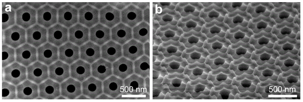
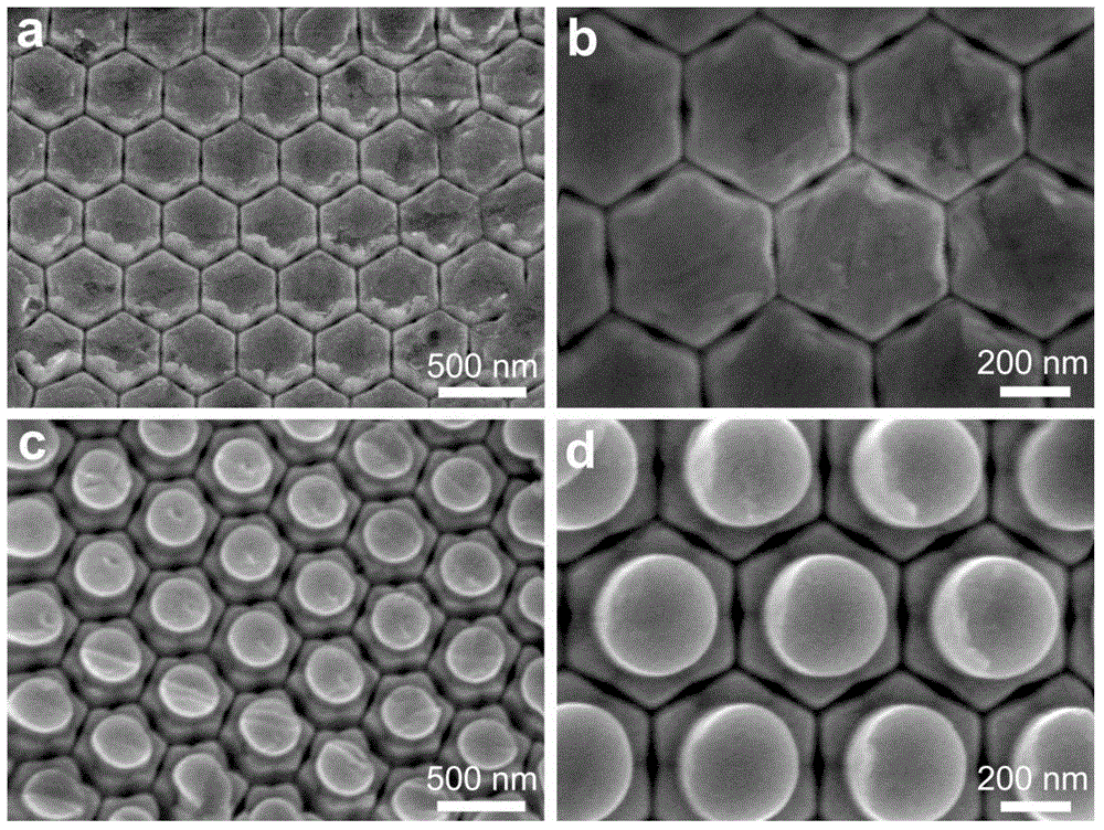
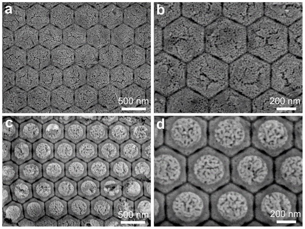
[0051] Step 1: First place the aluminum sheet in -1°C, 1.5wt% phosphoric acid solution, anodize it at 190V DC constant voltage for 4.5h, and then soak it in 55°C phosphochromic acid mixture for 11h. Next, put it again under the same process conditions for the second anodic oxidation for 13 hours, first remove the unoxidized aluminum on the back with a saturated tin chloride solution, and then place it in a 12wt% phosphoric acid solution at 48°C to remove After the barrier layer, the hole was expanded for 5 minutes to obtain a through-hole alumina template with a hole diameter of 160nm, a hole period of 470nm, and a hexagonal concave-convex structure array between the holes; wherein, the hexagonal concave-convex structure is formed by the outer wall of the hole and the surrounding pits, the hole The inner wall is formed between adjacent pits, the pits are all located at the hexagons of the hexagonal concave-convex structure, the t...

Embodiment 2

[0054] The concrete steps of preparation are:

[0055] Step 1: first place the aluminum sheet in 0°C, 1.3wt% phosphoric acid solution, anodize it at 193V DC constant voltage for 4.3h, and then soak it in 58°C phosphoric chromic acid mixture for 10.5h. Next, put it under the same process conditions for the second anodic oxidation for 13.5 hours, remove the unoxidized aluminum on the back with a saturated tin chloride solution, and then place it in an 11wt% phosphoric acid solution at 49°C After removing the barrier layer, the hole was expanded for 10 minutes to obtain a through-hole alumina template with a hole diameter of 215nm, a hole period of 478nm, and an array of hexagonal concave-convex structures between the holes; where the hexagonal concave-convex structure is formed by the outer wall of the hole and the surrounding pits, The inner wall formed between the adjacent pits between the holes is composed of the pits located at the hexagons of the hexagonal concave-convex st...

Embodiment 3

[0058] The concrete steps of preparation are:

[0059] Step 1: first place the aluminum sheet in a 1°C, 1wt% phosphoric acid solution, anodize it at a DC constant voltage of 195V for 4 hours, and then soak it in a phosphochromic acid mixture at 60°C for 10 hours. Then, put it again under the same process conditions for the second anodic oxidation for 14 hours, first remove the unoxidized aluminum on the back with a saturated tin chloride solution, and then place it in a 10wt% phosphoric acid solution at 50°C to remove After the barrier layer, the hole was expanded for 15 minutes to obtain a through-hole alumina template with a hole diameter of 270nm, a hole period of 486nm, and an array of hexagonal concave-convex structures between the holes; wherein, the hexagonal concave-convex structure is formed by the outer wall of the hole and the surrounding pits, the hole The inner wall is formed between the adjacent pits, the pits are all located at the hexagons of the hexagonal conc...


PUM

PropertyMeasurementUnit
diameteraaaaaaaaaa
widthaaaaaaaaaa
wavelengthaaaaaaaaaa

Abstract

The invention discloses an ordered nanostructured precious metal array, and a preparation method and a use thereof. The array is characterized in that projections with the height positioned in hexagons being not greater than 20nm are arranged at the column ends of a nanometer hexagonal prism for composing a gold-silver alloy nanometer hexagonal prism array or a porous gold nanometer hexagonal prism array, the column structure cycle of the nanometer hexagonal prism is 470-500nm, the column height of the nanometer hexagonal prism is 50-200nm, the column wall of the nanometer hexagonal prism has a concave arc shape, and the column gap of adjacent nanometer hexagonal prisms is 5-50nm. The method comprises the following steps: producing a through-hole alumina template with the hole diameter of 160-380nm, the hole cycle of 470-500nm and the hole gap of a hexagonal concave-convex structure array by using a two-stage anode oxidation technology, coating the through-hole alumina template as a die on a gold-silver alloy film or a porous gold film, and applying a pressure being not greater than 5.7*10<6>N/m<2> to the through-hole alumina template to prepare a target product. The ordered nanostructured precious metal array can be used as a surface enhanced Raman scattering active substrate, and the content of rhodamine or methyl parathion or polychlorinated biphenyl-3 adhered on the active substrate can be measured by using a laser Raman spectrometer.

Description

technical field [0001] The invention relates to an ordered nanostructure array, its preparation method and application, in particular to a precious metal ordered nanostructure array, its preparation method and application. Background technique [0002] In recent years, surface-enhanced Raman scattering (SERS) technology based on the electromagnetic field enhancement mechanism of gold, silver, copper and other noble metal nanostructures has the advantages of simplicity, speed, and high sensitivity, and can accurately reflect the fingerprint information of chemical and biomolecular structures. One of the compelling trace detection techniques. Theoretical and experimental studies have shown that the SERS effect mainly comes from the enhanced electromagnetic field generated between nanounits. When the gap between nanounits is less than 10nm, a strong local coupling electric field will be generated at the gap, which is usually called SERS "hot spot". Therefore, in order to obta...

Claims


Application Information

Patent Timeline
Patent Type & Authority Applications(China)
IPC IPC(8): G01N21/65C25B11/12B82Y30/00B82Y40/00
Inventor 陈斌孟国文黄竹林周飞
Owner HEFEI INSTITUTES OF PHYSICAL SCIENCE - CHINESE ACAD OF SCI
Why Eureka
Try Eureka