

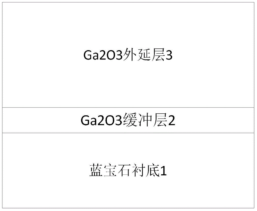
Gallium oxide film based on sapphire substrate and growing method of gallium oxide film
A sapphire substrate and gallium oxide technology, which is applied in the field of microelectronics, can solve the problems of poor surface morphology and small grain size of Ga2O3 films, and achieve the effects of improving surface morphology, improving crystal quality, and increasing coverage
- Summary
- Abstract
- Description
- Claims
- Application Information
AI Technical Summary
Problems solved by technology
Method used
Image

Examples
Embodiment 1
[0029] Example 1, a gallium oxide thin film with a buffer layer thickness of 7 nm was fabricated.
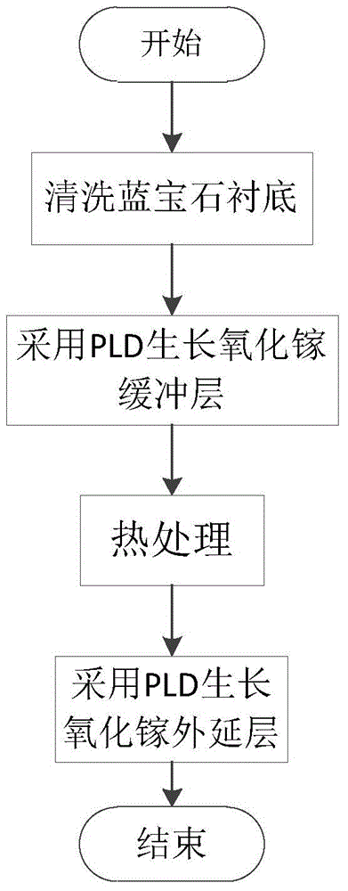
[0030] Step 1, cleaning the sapphire substrate.
[0031] (1a) Soak the sapphire substrate in a mixture of sulfuric acid and phosphoric acid for 30 minutes, the ratio of sulfuric acid and phosphoric acid is 3:1;
[0032] (1b) Clean the sapphire substrate with acetone and absolute ethanol for 6 min respectively;
[0033] (1c) Rinse the sapphire substrate with deionized water and blow dry with dry nitrogen.
[0034] Step 2, growing a gallium oxide buffer layer with a thickness of 7 nm.
[0035] (2a) Put the cleaned sapphire substrate into the pulsed laser deposition PLD chamber, and pump the vacuum degree of the pulsed laser deposition PLD chamber to 10 -6 mbar, the distance between the substrate and the gallium oxide target is adjusted to 50mm, and the speed of the target is kept at 30rpm;
[0036] (2b) Heat the sapphire substrate to 500°C, adjust the oxygen partial pressure i...
Embodiment 2
[0043] Example 2, making a gallium oxide thin film with a buffer layer thickness of 12nm.
[0044] The first step is to clean the sapphire substrate.
[0045] This step is the same as Step 1 of Example 1.
[0046] In the second step, a gallium oxide buffer layer with a thickness of 12nm is grown.
[0047] 2.1) Put the cleaned sapphire substrate into the pulsed laser deposition PLD chamber, and pump the vacuum degree of the pulsed laser deposition PLD chamber to 10 -6 mbar, the distance between the substrate and the gallium oxide target is adjusted to 50mm, and the speed of the target is kept at 30rpm;
[0048] 2.2) Heat the sapphire substrate to 570°C, adjust the oxygen partial pressure in the pulsed laser deposition PLD chamber to 0.015mbar, set the laser energy to 450mJ, the laser frequency to 3Hz, and the number of pulses to 1600 to grow the Ga2O3 buffer layer;
[0049] 2.3) After the growth of the buffer layer is completed, the pulsed laser deposition PLD chamber is fil...
Embodiment 3
[0060] Example 3, making a gallium oxide thin film with a buffer layer thickness of 10 nm.
[0061] Step A, cleaning the sapphire substrate.
[0062] The implementation of this step is the same as step 1 in Embodiment 1.
[0063] Step B, growing a gallium oxide buffer layer with a thickness of 10 nm.
[0064] (B1) Put the cleaned sapphire substrate into the pulsed laser deposition PLD chamber, and pump the vacuum degree of the pulsed laser deposition PLD chamber to 10 -6 mbar, the distance between the substrate and the gallium oxide target is adjusted to 50mm, and the speed of the target is kept at 30rpm;
[0065] (B2) Heating the substrate to 600°C, adjusting the oxygen partial pressure in the pulsed laser deposition PLD chamber to 0.02mbar, setting the laser energy to 460mJ, the laser frequency to 3Hz, and the number of pulses to 1400 to grow a Ga2O3 buffer layer;
[0066] (B3) After the growth of the buffer layer is completed, 200 mbar of oxygen is filled into the pulsed...
PUM
| Property | Measurement | Unit |
|---|---|---|
| Thickness | aaaaa | aaaaa |
| Thickness | aaaaa | aaaaa |
| Thickness | aaaaa | aaaaa |
Abstract
Description
Claims
Application Information