Back surface junction N-type double-sided crystal silicon cell and preparation method thereof

A crystalline silicon cell, N-type technology, applied in circuits, electrical components, photovoltaic power generation, etc., can solve the problems of increasing impurity concentration of silicon substrate, reducing production cost, reducing surface doping concentration, etc., to reduce etching and masking. The process of film deposition, the effect of reducing the cost of the production process, and reducing the rate of interfacial recombination

Inactive Publication Date: 2015-12-30
中国东方电气集团有限公司
View PDF4 Cites 14 Cited by
  • Summary
  • Abstract
  • Description
  • Claims
  • Application Information

AI Technical Summary

Problems solved by technology

This high temperature process will easily lead to changes in the diffusion curve of the p+ layer, such as the decrease of the surface doping concentration and the increase of the junction depth, resulting in an increase in the series resistance of the battery and a decrease in electrical contact performance; at the same time, the high temperature process will easily lead to an increase in the impurity concentration of the silicon substrate , the bulk recombination of the battery will intensify, and finally manifest as a decrease in the open circuit voltage and overall efficiency
Patent CN102544236B reports that after completing single-sided B doping to form a p+ boron emitter layer, the borosilicate glass layer is removed, and then SiN is deposited on both sides of the silicon wafer by low-pressure chemical vapor deposition (LPCVD) x film, and then expand the SiN surface on the B x SiO deposited on 2 , using phosphoric acid to remove uncoated SiO 2 Protected SiN x surface, and then perform phosphorus diffusion on this surface. This method involves multiple coating and cleaning processes. The process is relatively complicated, which is not conducive to improving production efficiency and reducing production costs.

Method used


Image

  • Back surface junction N-type double-sided crystal silicon cell and preparation method thereof
  • Back surface junction N-type double-sided crystal silicon cell and preparation method thereof

Examples


Embodiment 1

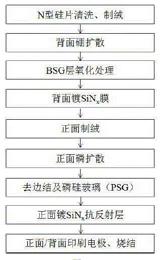
[0027] Such as figure 2 Shown, a kind of preparation method of rear junction N-type double-sided crystalline silicon solar cell comprises the following steps:

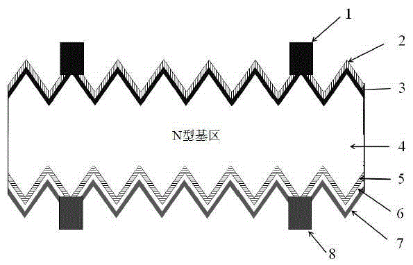
[0028] (1) Using N-type monocrystalline silicon as the substrate, the silicon wafer is cleaned and textured. The resistivity of the N-type monocrystalline silicon substrate is 1~12Ω·cm, and the thickness is 170~200mm;

[0029] (2) Place the front side of the above-mentioned silicon wafer face-to-face for single-sided boron diffusion, the back of the silicon wafer is the boron diffusion surface, and the sheet resistance is 60Ω / □, using BBr 3 Liquid source diffusion, the diffusion temperature is 970 degrees, and the time is 60 minutes;

[0030] (3) During the cooling process after the boron diffusion propulsion is completed, a certain flow of oxygen is introduced to oxidize the borosilicate glass and its interface with silicon until the temperature is lowered to 790°C. The flow rate of oxygen is 3-16slm, preferably 10s...

Embodiment 2

[0039] Such as figure 2 Shown, a kind of preparation method of rear junction N-type crystalline silicon solar cell comprises the steps:

[0040] (1) Using N-type monocrystalline silicon as the substrate, the silicon wafer is cleaned and textured. The resistivity of the N-type monocrystalline silicon substrate is 1~12Ω·cm, and the thickness is 170~200mm;

[0041] (2) Place the front side of the above-mentioned silicon chip face-to-face for single-sided boron diffusion. 3 Liquid source diffusion, the diffusion temperature is 930°C, and the time is 60min;

[0042] (3) During the cooling process after the boron diffusion propulsion is completed, a certain flow rate of oxygen is introduced to oxidize the borosilicate glass and its interface with silicon until the temperature is lowered to 790°C, the flow rate of oxygen is 5slm, and the oxidation time is 10min;

[0043] (4) Deposit a layer of silicon nitride film on the oxidized borosilicate glass layer by plasma enhanced chemica...


PUM

PropertyMeasurementUnit
thicknessaaaaaaaaaa
thicknessaaaaaaaaaa
thicknessaaaaaaaaaa

Abstract

The invention provides a back surface junction N-type double-sided crystal silicon cell and a preparation method thereof. The cell comprises a front surface Ag electrode, a front surface antireflection film, a phosphorus diffusion N+ front surface field layer, an N-type substrate, a boron diffusion emission electrode P+ layer, a back surface passivation composite film and a back surface AgAl electrode. The front surface and the back surface of the cell have a textured structure. The back surface passivation composite film comprises a borosilicate glass layer and a silicon nitride layer. The borosilicate glass layer is arranged on the boron diffusion emission electrode P+ layer. The silicon nitride layer is deposited on the borosilicate glass layer. Both of the front surface and the back surface of the cell can effectively receive sunlight irradiation for power generation so that comprehensive efficiency of the cell can be enhanced; and the laminated film of the borosilicate glass layer and the silicon nitride layer through oxidation treatment is adopted to act as a boron emission electrode passivation layer and a diffusion masking layer of subsequent phosphorus diffusion so that boron emission electrode passivation and diffusion masking functions can be realized simultaneously, and the process of multiple times of etching and mask deposition in the manufacturing process can be reduced. The back surface junction N-type double-sided crystal silicon cell is simple in technology, high in production efficiency and low in production technology cost.

Description

technical field [0001] The invention relates to the technical field of solar cell production, in particular to a rear junction N-type double-sided crystal silicon cell and a preparation method thereof. Background technique [0002] At present, crystalline silicon cells are the mainstream products in the solar cell market, and crystalline silicon solar cells can be divided into P-type crystalline silicon cells and N-type crystalline silicon cells in terms of material and substrate types. Compared with P-type monocrystalline silicon cells, N-type monocrystalline silicon cells have the characteristics of small light-induced attenuation, good resistance to metal impurity pollution, and long minority carrier diffusion length. This is because (1) The light-induced attenuation effect of the P-type cell is caused by the combination of boron and oxygen in the P-type crystalline silicon substrate. There are boron and oxygen in the medium, and using N-type crystalline silicon instead ...

Claims


Application Information

Patent Timeline
Patent Type & Authority Applications(China)
IPC IPC(8): H01L31/068H01L31/0216H01L31/18
CPCH01L31/02168H01L31/0682H01L31/0684H01L31/1804Y02E10/547Y02P70/50
Inventor 张中伟李愿杰黄仑
Owner 中国东方电气集团有限公司
Why Eureka
Try Eureka