Technology for sealing micropore opening

A microporous and open technology, applied in the field of semiconductor technology, can solve the problems of difficult control of film thickness uniformity, high operating cost, low deposition rate, etc., and achieve the effects of rich and diverse shapes, convenient processing, and high specific surface area

Active Publication Date: 2016-02-17
CHONGQING INST OF GREEN & INTELLIGENT TECH CHINESE ACADEMY OF SCI
View PDF2 Cites 2 Cited by
  • Summary
  • Abstract
  • Description
  • Claims
  • Application Information

AI Technical Summary

Problems solved by technology

In these methods, the deposition process of the hole starts from both sides of the hole wall to the center, and there is no report on the method of depositing and sealing the hole above the hole.
And the atomic layer deposition process is discontinuous, complex surface chemical process and low deposition rate; in the sol-gel method, there is a large amount of liquid in the gel, which is prone to cracking and large shrinkage during the drying process of the film, and the film thickness is uniform The property is difficult to control; the organic solvent is toxic, harmful to the human body and pollutes the environment; the process cycle is long; the thickness of the coating obtained by sputtering is uneven, the device is too complicated, the deposition rate is low, and the operating cost is high

Method used


Image

  • Technology for sealing micropore opening
  • Technology for sealing micropore opening
  • Technology for sealing micropore opening

Examples


Embodiment 1

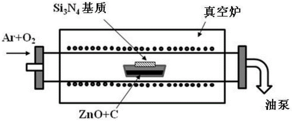
[0031] 1) Mix and grind ZnO powder and carbon powder at a mass ratio of 1:1, and place the powder in a corundum boat;

[0032] 2) In Si containing micropores with a diameter of 5 μm 3 N 4 The area around the holes of the substrate is sputtered with an appropriate amount of Au, the Si3N4 substrate containing micropores is placed on a corundum boat, and the micropores are exposed to the mixed powder;

[0033] 3) Place the corundum boat at the center of the tube furnace of the chemical vapor deposition equipment, evacuate the gas chamber, and increase the temperature of the tube furnace at a rate of 15 °C / min. When the temperature rises to 600 °C, the carrier gas Ar and O 2 Mix at a ratio of 100sccm: 1.5sccm while passing it into the gas chamber, keep the growth pressure at 30KPa, stop the temperature rise after the temperature rises to 960°C, and maintain this condition for 20 minutes of deposition.

Embodiment 2

[0038] 1) Mix and grind ZnO powder and carbon powder at a mass ratio of 1:1, and place the powder in a corundum boat;

[0039] 2) In Si containing micropores with square pores with a side length of 35 μm 3 N 4 The area around the hole of the substrate is sputtered with an appropriate amount of Au, which will contain microporous Si 3 N 4The substrate is placed on the corundum boat with the opening of the pores facing the mixed powder;

[0040] 3) Place the corundum boat at the center of the tube furnace of the chemical vapor deposition equipment, evacuate the gas chamber, and increase the temperature of the tube furnace at a rate of 15 °C / min. When the temperature rises to 600 °C, the carrier gas Ar and O 2 Mix at a ratio of 100sccm: 1.5sccm while passing it into the air chamber, keep the growth pressure stable at 30KPa, stop the temperature rise after the temperature rises to 900°C and keep this condition for deposition for 20min, 30min, 40min.

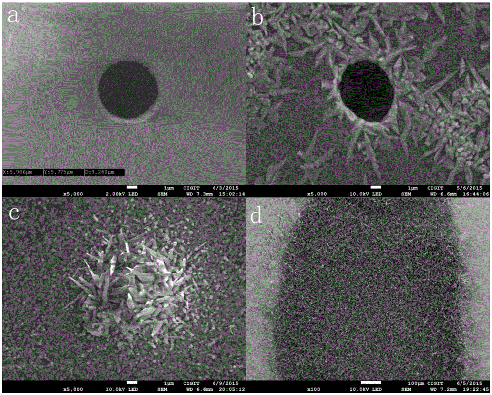
[0041] image 3 Represent...

Embodiment 3

[0043] 1) Mix and grind ZnO powder and carbon powder at a mass ratio of 1:1, and place the powder in a corundum boat;

[0044] 2) In Si containing micropores with square pores with a side length of 450 μm 3 N 4 The area around the holes of the substrate is sputtered with an appropriate amount of Au, the Si3N4 substrate containing micropores is placed on a corundum boat, and the micropores are exposed to the mixed powder;

[0045] 3) Place the corundum boat at the center of the tube furnace of the chemical vapor deposition equipment, evacuate the gas chamber, and increase the temperature of the tube furnace at a rate of 15 °C / min. When the temperature rises to 600 °C, the carrier gas Ar and O 2 Mix at a ratio of 100sccm: 1.5sccm while feeding into the gas chamber, keep the growth pressure stable at 30KPa, stop the temperature rise after the temperature rises to 1000°C, and maintain this condition for deposition for 20min and 50min.

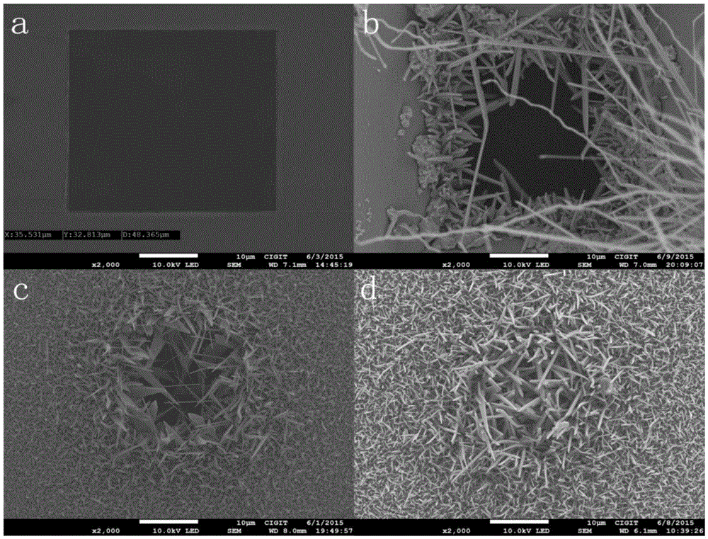
[0046] Figure 4 Represents the SEM image...


PUM


Abstract

The invention discloses a technology for sealing a micropore opening. A ZnO nanometer structure is prepared on a Si3N4 substrate with a micrometer pore by utilizing a Au catalysis assisted chemical vapor deposition growth technology, and the purpose of surface sealing is realized. In the hole sealing process, planar deposition is performed from the pore wall to the pore center, the deposition rate of the micropore surface is controlled by controlling the deposition temperature and time, and finally a zinc oxide film is formed. The zinc oxide film comprises a zinc oxide nano-wire layer composed of crosswise-grown zinc oxide nano-wires, nano-sheets or nano-columns, and the formed nanometer material structure is definite and ordered, a high specific surface area can be realized. Si3N4 subjected to hole-sealing processing can be taken as a bearing, wave transmission and heat-protection material, and is applicable to the technical field of semiconductor nanometer materials, and the ZnO nanometer structure with multiple forms is easy to etch, thereby facilitating the subsequent technology for processing.

Description

technical field [0001] The invention belongs to the technical field of semiconductor technology, in particular to a technology for sealing micropore openings by chemical vapor deposition of ZnO nanometer layers. Background technique [0002] As a typical n-type, II-VI direct bandgap, wide bandgap (Eg about 3.37eV at room temperature) semiconductor material, ZnO is suitable for the application of short-wave and short-wave optoelectronic devices. Unlike other wide bandgap semiconductors, its room temperature The lower exciton binding energy is as high as 60meV, which is 2.4 times that of the thermal ionization energy (26meV) at room temperature, and the excitons will not be thermally ionized at room temperature. At room temperature, ZnO micro-nano materials have attracted much attention due to their good electrical and thermal conductivity, unique piezoelectric, pyroelectric and photoelectric properties, and excellent biocompatibility. Based on these properties, it is conside...

Claims


Application Information

Patent Timeline
IPC IPC(8): C04B41/85
CPCC04B41/009C04B41/5049C04B41/85C04B2111/00008C04B41/4531C04B35/584
Inventor 王德强赵越陆文强崔洪亮杜春雷
Owner CHONGQING INST OF GREEN & INTELLIGENT TECH CHINESE ACADEMY OF SCI
Why Eureka
Try Eureka