OFET (Organic Field Effect Transistor) ammonia gas sensor containing functional insulation layer
A technology of ammonia sensor and functional insulation, applied in the direction of instruments, scientific instruments, measuring devices, etc., can solve the problems of difficult realization of flexibility, large-area devices, few applications, environmental pollution, etc., and achieve green and pollution-free detection in the preparation process Effectively improve the performance and improve the effect of gas-sensing characteristics
- Summary
- Abstract
- Description
- Claims
- Application Information
AI Technical Summary
Problems solved by technology
Method used
Image
Examples
Embodiment 1
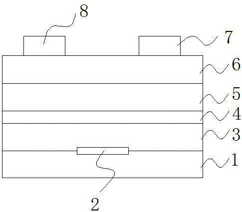
[0030] Such as figure 1 The bottom-gate-top-contact structure is shown, and the materials and thicknesses of each layer are as follows: substrate 1 is glass, gate electrode 2 is aluminum with a thickness of 30nm, and insulating layer a3 is polymethyl methacrylate with a thickness of 100nm. The insulating layer 4 is polyvinyl alcohol with a thickness of 30nm, the insulating layer b5 is polymethyl methacrylate with a thickness of 100nm, the organic semiconductor layer 6 is copper phthalocyanine with a thickness of 30nm, the source electrode and the drain electrode 7 are both Au, The thickness is 30nm.
[0031] The preparation method is as follows:
[0032] ① Thoroughly clean the substrate 1, and dry it with dry nitrogen after cleaning;
[0033] ② Sputtering the gate electrode on the surface of the substrate 1;
[0034] ③ Spin-coating an insulating layer a on the gate electrode;
[0035] ④ Prepare a functional insulating layer on the insulating layer a by spin coating;
[00...
Embodiment 2
[0040] Such as figure 1 The bottom gate top contact structure is shown, the material and thickness of each layer are: substrate 1 is glass, gate electrode 2 is ITO, the thickness is 80nm, the insulating layer a3 is polymethyl methacrylate, the thickness is 200nm, the function The insulating layer 4 is polyvinyl alcohol with a thickness of 50nm, the insulating layer b5 is polymethyl methacrylate with a thickness of 200nm, the organic semiconductor layer 6 is pentacene with a thickness of 50nm, the source electrode and the drain electrode 7 are both Au, The thickness is 80nm.
[0041] Preparation method is like embodiment 1.
Embodiment 3
[0043] Such as figure 1The bottom-gate-top-contact structure is shown, and the material and thickness of each layer are as follows: substrate 1 is glass, gate electrode 2 is ITO with a thickness of 50nm, and insulating layer a3 is polymethyl methacrylate with a thickness of 200nm. The insulating layer 4 is polyvinyl alcohol with a thickness of 50nm, the insulating layer b5 is polystyrene with a thickness of 200nm, the organic semiconductor layer 6 is pentacene with a thickness of 50nm, and the source electrode and drain electrode 7 are Au with a thickness of 80nm .
[0044] Preparation method is like embodiment 1.
PUM
| Property | Measurement | Unit |
|---|---|---|
| thickness | aaaaa | aaaaa |
| thickness | aaaaa | aaaaa |
| thickness | aaaaa | aaaaa |
Abstract
Description
Claims
Application Information

