LED epitaxial structure and manufacturing method thereof
A technology of epitaxial structure and manufacturing method, which can be used in electrical components, circuits, semiconductor devices, etc., and can solve problems such as low VF.
- Summary
- Abstract
- Description
- Claims
- Application Information
AI Technical Summary
Problems solved by technology
Method used
Image
Examples
Embodiment 1
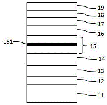
[0041] Please refer to figure 1 , the present embodiment provides an LED epitaxial structure, including from bottom to top: a substrate 11, a buffer layer 12, a first conductivity type semiconductor layer including a U-GaN layer 13 and an N-GaN layer 14, and a low Al Component Al x Ga 1-x The stress release layer 15 of the N layer 151 (0.1%≤x≤1%), the quantum well layer 16, and the second conductivity type semiconductor layer including the electron blocking layer 17, the P-GaN layer 18 and the contact layer 19, wherein the stress release layer A GaN layer or an InGaN / GaN superlattice layer can be selected, and the GaN layer is preferred in this embodiment.
[0042] Specifically, the substrate 11 of this embodiment is selected from sapphire (Al 2 o 3 ), at least one of SiC, GaAs, GaN, ZnO, Si, GaP, InP and Ge, preferably a flat sapphire substrate, although not shown in the figure, the sapphire substrate can also be a patterned sapphire substrate ( PSS), therefore, embodime...
Embodiment 2
[0049] Please refer to figure 1 , the present embodiment provides a method for manufacturing an LED epitaxial structure, including the following process steps:
[0050] (1) Provide a substrate 11, preferably a patterned sapphire substrate (PSS), put it into a metal-organic chemical vapor deposition (MOCVD) device and raise the temperature to 1000-1200°C, and process it in a hydrogen atmosphere for 3-10 minutes.
[0051] (2) Cool down to 500~600°C, feed ammonia gas and trimethylgallium, epitaxially grow a low-temperature buffer layer 12 of 20~50nm on the substrate 11, preferably InAlGaN semiconductor material, to play the role of stress release, and then shut down Sanjia Potassium Gallium; the epitaxial growth method can also choose CVD (Chemical Vapor Deposition) method, PECVD (Plasma Enhanced Chemical Vapor Deposition) method, MBE (Molecular Beam Epitaxy) method, HVPE (Hydride Vapor Phase Epitaxy) method, preferably MOCVD, But the embodiment is not limited thereto.
[0052]...
Embodiment 3
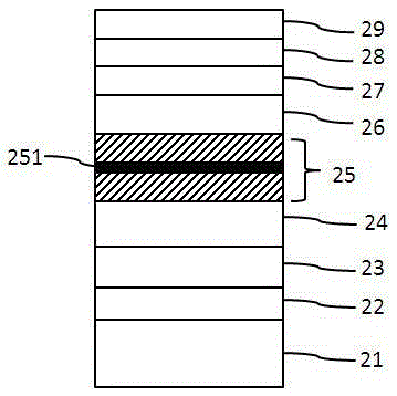
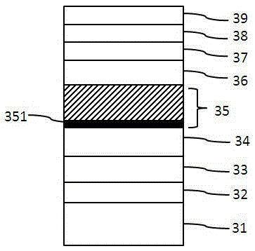
[0057] Please refer to figure 2 , the difference from Embodiment 1 is that the stress release layer 25 of this embodiment is an InGaN / GaN superlattice layer with 10 to 30 cycles, the thickness of InGaN in each cycle ranges from 1 to 3 nm, and the thickness of GaN ranges from 2 nm to 2 nm. ~8nm, the overall thickness is controlled between 50~400nm; the AlGaN insertion layer with low aluminum composition can be inserted between any period of the InGaN / GaN superlattice layer, and can also be inserted into each period of the InGaN / GaN superlattice Inside the layer; the number of AlGaN insertion layers can be single or N (N is a natural number of 2≤N≤30). In this embodiment, a single AlGaN layer 251 is preferably inserted between any period of the InGaN / GaN superlattice layer.
PUM
 Abstract
Description
Claims
Application Information
 - R&D
- Intellectual Property
- Life Sciences
- Materials
- Tech Scout
- Unparalleled Data Quality
- Higher Quality Content
- 60% Fewer Hallucinations
Browse by: Latest US Patents, China's latest patents, Technical Efficacy Thesaurus, Application Domain, Technology Topic, Popular Technical Reports.
© 2025 PatSnap. All rights reserved.Legal|Privacy policy|Modern Slavery Act Transparency Statement|Sitemap|About US| Contact US: help@patsnap.com


