

Preparation method for ZnO nanocrystalline thin-film transistor type UV detector
A thin film transistor and ultraviolet detector technology, which is applied in nanotechnology, nanotechnology, semiconductor devices, etc., can solve the problems of unseen thin film transistor ultraviolet detectors, etc., and achieves high electron transmission speed, simple preparation method and high yield. Effect
- Summary
- Abstract
- Description
- Claims
- Application Information
AI Technical Summary
Problems solved by technology
Method used
Image

Examples
Embodiment 1
[0023] 1) Weigh 0.6585g of Zn(CH 3 COOH) 2 2H 2 O was dissolved in 30mL dimethyl sulfoxide to obtain A solution;
[0024] Weigh 0.9968g of (CH 3 ) 4 NOH·5H 2 O was dissolved in 10mL ethanol to obtain solution B;
[0025] Slowly add the B solution to the A solution, and stir the reaction at room temperature for 2 hours to obtain the mixed solution C;
[0026] Add 40mL of ethyl acetate to solution C to precipitate ZnO nanocrystals, pour off the supernatant after centrifugation, add 10mL ethanol and 160uL ethanolamine to dissolve ZnO nanocrystals, then add 20mL ethyl acetate to precipitate ZnO nanocrystals, centrifuge Then pour off the supernatant, finally add 2mL of ethanol, and filter with a 0.22um PTFE filter head to obtain a colloidal dispersed phase of ZnO nanocrystals.
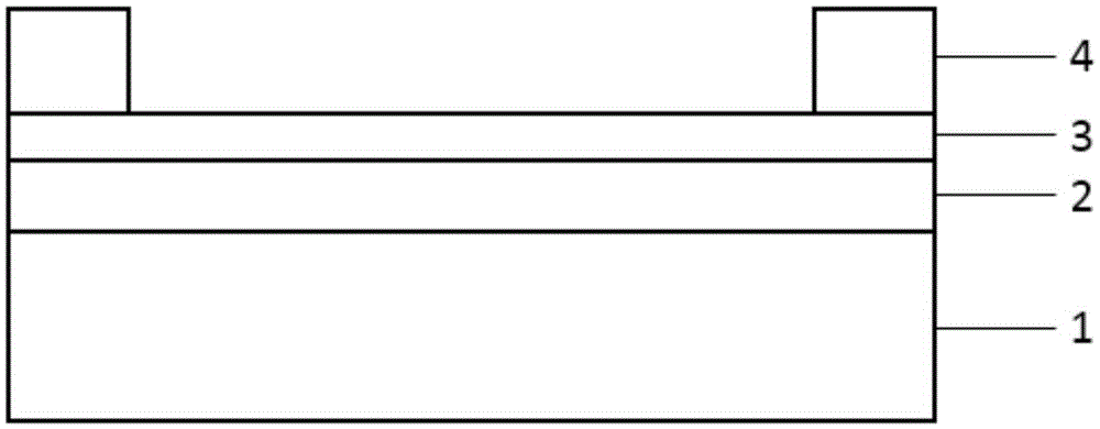
[0027] 2) Prepare SiO with a thickness of 300nm on a clean low-resistance Si sheet (1) with a resistivity of 0.001-0.005Ω·cm 2 insulating layer (2), again in SiO 2 The ZnO nanocrystalline colloidal...
Embodiment 2
[0031] 1) Weigh 0.6585g of Zn(CH 3 COOH) 2 2H 2 O was dissolved in 30mL dimethyl sulfoxide to obtain A solution;
[0032] Weigh 0.9968g of (CH 3 ) 4 NOH·5H 2 O was dissolved in 10mL ethanol to obtain solution B;
[0033] Slowly add the B solution to the A solution, and stir the reaction at room temperature for 2 hours to obtain the mixed solution C;
[0034] Add 40mL of ethyl acetate to solution C to precipitate ZnO nanocrystals, pour off the supernatant after centrifugation, then add 10mL ethanol and 160uL ethanolamine to dissolve ZnO nanocrystals, then add 50mL ethyl acetate to precipitate ZnO nanocrystals, centrifuge Finally, the supernatant was poured off, and finally 4 mL of ethanol was added, and the colloidal dispersed phase of ZnO nanocrystals was obtained after filtering with a 0.22 um PTFE filter head.
[0035] 2) Prepare SiO with a thickness of 300nm on a clean low-resistance Si sheet (1) with a resistivity of 0.001-0.005Ω·cm 2 insulating layer (2), again in...
Embodiment 3
[0039] 1) Weigh 0.6585g of Zn(CH 3 COOH) 2 2H 2 O was dissolved in 30mL dimethyl sulfoxide to obtain A solution;
[0040] Weigh 0.9968g of (CH 3 ) 4 NOH·5H 2 O was dissolved in 10mL ethanol to obtain solution B;
[0041] Slowly add the B solution to the A solution, and stir the reaction at room temperature for 24 hours to obtain the mixed solution C;
[0042]Add 40mL of ethyl acetate to solution C to precipitate ZnO nanocrystals, pour off the supernatant after centrifugation, then add 10mL ethanol and 160uL ethanolamine to dissolve ZnO nanocrystals, then add 50mL ethyl acetate to precipitate ZnO nanocrystals, centrifuge Finally, the supernatant was poured off, and finally 4 mL of ethanol was added, and the colloidal dispersed phase of ZnO nanocrystals was obtained after filtering with a 0.22 um PTFE filter head.
[0043] 2) Prepare SiO with a thickness of 300nm on a clean low-resistance Si sheet (1) with a resistivity of 0.001-0.005Ω·cm 2 insulating layer (2), again in...
PUM
| Property | Measurement | Unit |
|---|---|---|
| Thickness | aaaaa | aaaaa |
Abstract
Description
Claims
Application Information