Method for increasing ohmic contact characteristic of silicon carbide semiconductor

An ohmic contact and silicon carbide technology, applied in the field of microelectronics, can solve the problems of poor thermal stability and process compatibility, high preparation cost, and achieve the effect of reducing surface state density, low barrier height, and improving ohmic contact characteristics.

Inactive Publication Date: 2016-06-22
DALIAN UNIV OF TECH
View PDF3 Cites 15 Cited by
  • Summary
  • Abstract
  • Description
  • Claims
  • Application Information

AI Technical Summary

Problems solved by technology

This method not only does not require high-temperature annealing, but also avoids the use of heavily doped silicon carbide substrates, which solves the problems of high preparation costs, thermal stability and low Problems such as poor process compatibility can reduce the cost of silicon carbide device preparation and improve device reliability

Method used


Image

  • Method for increasing ohmic contact characteristic of silicon carbide semiconductor
  • Method for increasing ohmic contact characteristic of silicon carbide semiconductor
  • Method for increasing ohmic contact characteristic of silicon carbide semiconductor

Examples


Embodiment Construction

[0029] The present invention will be further described below in conjunction with accompanying drawing.

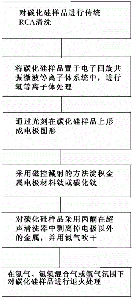
[0030] Such as figure 1 As shown, a method for improving the ohmic contact characteristics of a silicon carbide semiconductor comprises the following steps:

[0031] Step 1. Carry out traditional RCA cleaning on the silicon carbide sample, which specifically includes the following sub-steps:

[0032] (a) Clean the silicon carbide sample with deionized water and ultrasonic until there is no obvious foreign matter;

[0033] (b) using concentrated sulfuric acid (H 2 SO 4 ) cleaning, the H 2 SO 4 Heat to 80°C, boil for 10 minutes, put in the cleaned silicon carbide sample, soak for 30 minutes, add H 2 o 2 Soak for another 15 minutes, rinse the silicon carbide sample several times with deionized water;

[0034] (c) Use No. 1 standard solution (deionized water, NH 4 OH and H 2 o 2 Mixed solution) cleaning, DIW cleaning several times, buffered hydrofluoric acid cleaning...


PUM


Abstract

The invention relates to the field of microelectronic technology, a method for improving the ohmic contact characteristics of a silicon carbide semiconductor, comprising the following steps: (1) performing traditional RCA cleaning on a silicon carbide sample; (2) placing the silicon carbide sample in electron cyclotron resonance microwave plasma In the bulk system, hydrogen plasma treatment is carried out; (3) electrode pattern is formed on the silicon carbide sample by photolithography; (4) metal electrode material titanium or titanium carbide is deposited by magnetron sputtering; (5) The silicon sample was stripped of metal other than the electrodes in an ultrasonic cleaner with acetone, and dried with nitrogen; (6) the silicon carbide sample was annealed in a nitrogen atmosphere. In the present invention, after pre-treating the surface of silicon carbide with hydrogen plasma generated by an electron cyclotron resonance system, the surface of silicon carbide is effectively cleaned and passivated, and the surface state density is significantly reduced, and combined with low work function metal titanium or titanium carbide and relatively The silicon carbide substrate with high doping concentration has a low barrier height of Ti/SiC contact, and good ohmic contact can be formed under low temperature annealing conditions.

Description

technical field [0001] The invention relates to a method for improving the ohmic contact characteristics of a silicon carbide semiconductor, belonging to the technical field of microelectronics. Background technique [0002] At present, silicon carbide semiconductors have been widely used in the fields of high-temperature, high-frequency, and high-power electronic devices due to their large band gap, critical breakdown electric field, and high thermal conductivity. Silicon carbide devices have become the most advanced in the field of semiconductors. One of the hotspots and frontier areas of concern. The ohmic contact is the part of any semiconductor device connected to external components and circuit components. Low resistance and high stability ohmic contact are decisive factors for whether silicon carbide can be applied to high-temperature and high-power devices. Because working under high current density, small resistance will generate very large power consumption, while...

Claims


Application Information

Patent Timeline
Patent Type & Authority Applications(China)
IPC IPC(8): H01L29/24H01L29/45
CPCH01L29/24H01L29/401H01L29/45
Inventor 王德君秦福文黄玲琴李青洙
Owner DALIAN UNIV OF TECH
Why Eureka
Try Eureka