High quality perovskite thin film, solar cell and preparation method thereof
A technology for preparing solar cells and thin films, applied in the field of solar cells, can solve problems such as disadvantageous preparation of large-area thin films, increased process manufacturing costs, incomplete conversion of raw materials, etc., and achieves high uniformity, fewer defects, operability and reliability Strong control effect
- Summary
- Abstract
- Description
- Claims
- Application Information
AI Technical Summary
Problems solved by technology
Method used
Image
Examples
Embodiment 1
[0053] Embodiment 1: Use the method of the present invention to prepare high-quality perovskite film
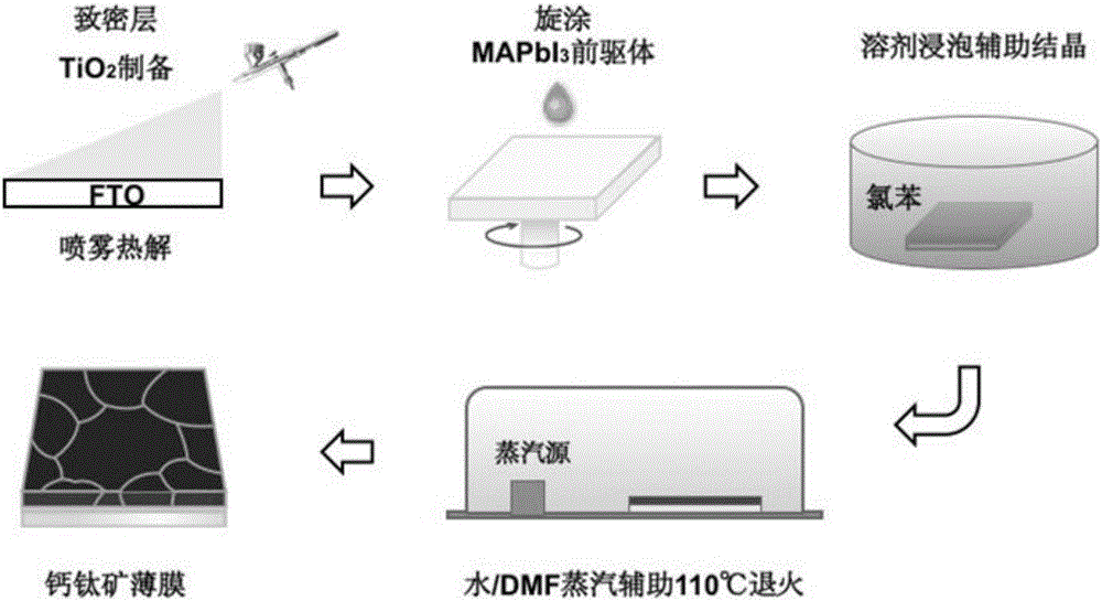
[0054] Choose PbI 2 And iodomethylamine is the precursor raw material of perovskite-type materials, which is dissolved in the mixed solvent of DMSO and DMF with a volume ratio of 1:1 according to the molar ratio of 1mmol:1mmol, and is configured to obtain a 45wt% precursor solution. The solution was spin-coated on the substrate at a spin-coating speed of 5000 rpm to obtain a yellow transparent film.
[0055] The film was soaked in chlorobenzene solvent, and after 120s, it was taken out and dried.
[0056] Then, placed in a mixed solvent vapor of deionized water and DMF with a volume ratio of 2%, and steam-assisted baking at 110° C. for 20 minutes to obtain the high-quality perovskite layer film of the present invention.
[0057] figure 1 A schematic diagram of a simple process flow for preparing high-quality perovskite films using the method of the present invention.
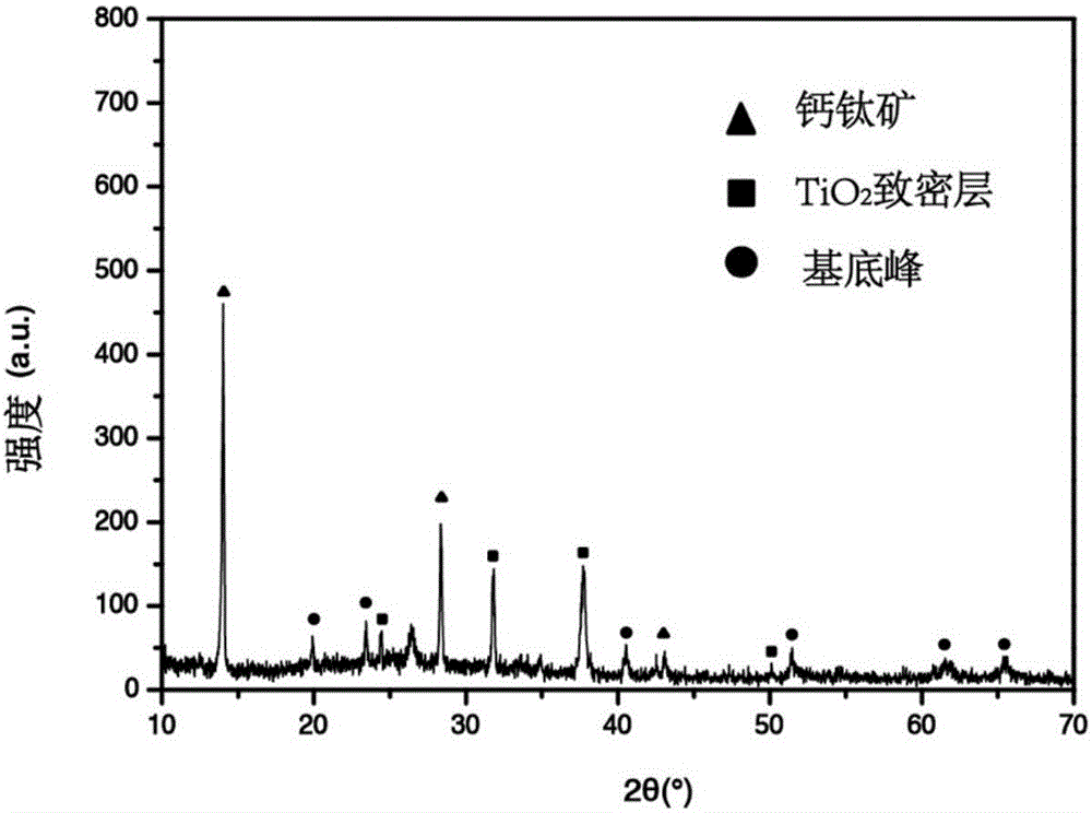
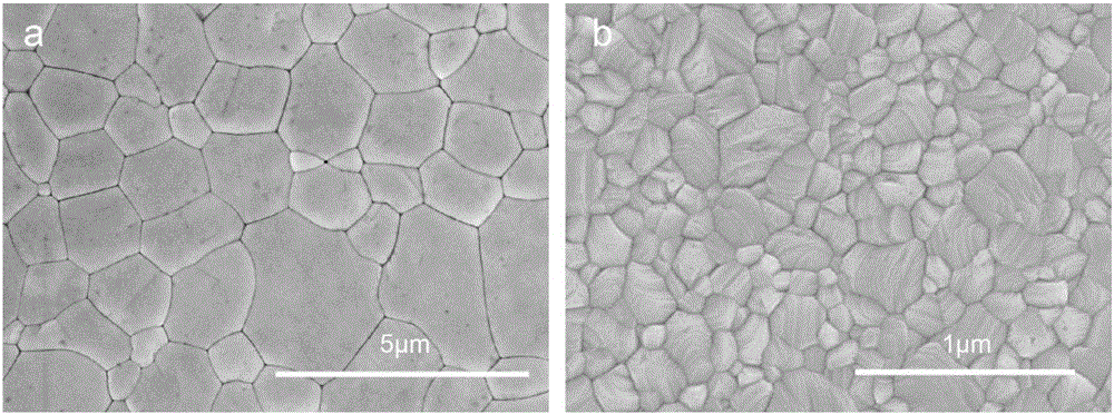
[0...
Embodiment 2
[0061] Embodiment 2: Preparation and performance testing of solar cell devices using high-quality perovskite thin films prepared by the method of the present invention
[0062] Using spray pyrolysis technology, the volume ratio of spray pyrolysis is 1:1 on the clean commercial transparent conductive substrate FTO (the thickness of the coating is about 250nm-300nm, the square resistance of the substrate is about 14Ω / □, and the light transmittance is 90%). Mixed precursor solution of titanium isopropoxybisacetylacetonate and ethanol. Then sintered at 500°C for 60 minutes to form TiO 2 dense layer.
[0063] According to the method described in Example 1, a high-quality perovskite film was prepared on the above substrate as a light-absorbing layer.
[0064] A hole transport layer Spiro-OMeTAD was prepared on the perovskite thin film (light absorbing layer) by spin coating.
[0065] A gold layer with a thickness of 80 nm was prepared as the top electrode of the device by vacuum ...
Embodiment 3
[0068] The perovskite film and device were prepared according to the same method as in Examples 1 and 2, except that the mixed solvent vapor of deionized water and DMF was used at a volume ratio of 4%. Tests show that its photoelectric conversion efficiency is 15.70%.
PUM
| Property | Measurement | Unit |
|---|---|---|
| Thickness | aaaaa | aaaaa |
| Particle size | aaaaa | aaaaa |
| Particle size | aaaaa | aaaaa |
Abstract
Description
Claims
Application Information


