Silicon carbide epitaxial growth system and growth method thereof

An epitaxial growth, silicon carbide technology, applied in chemical instruments and methods, crystal growth, single crystal growth and other directions, can solve the problems of inability to grow thick films, single system, etc., to achieve fewer defects, simple growth methods, and good process repeatability Effect

Pending Publication Date: 2016-08-17
GLOBAL ENERGY INTERCONNECTION RES INST CO LTD +2
View PDF6 Cites 6 Cited by
  • Summary
  • Abstract
  • Description
  • Claims
  • Application Information

AI Technical Summary

Problems solved by technology

However, the traditional SiC epitaxial growth system is single, can only grow in a slow growth mode, cannot grow thick films, and cannot meet the needs of high-voltage power electronic devices. Epitaxial growth system

Method used


Image

  • Silicon carbide epitaxial growth system and growth method thereof
  • Silicon carbide epitaxial growth system and growth method thereof
  • Silicon carbide epitaxial growth system and growth method thereof

Examples


Embodiment 1

[0041] a N + A method for preparing an NP-type silicon carbide epitaxial wafer with a low defect thickness, comprising the following steps:

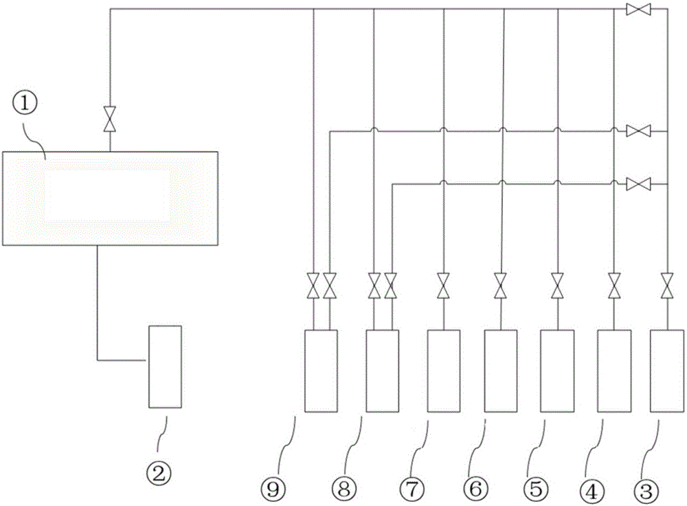
[0042] 1) Heating and heating: fill the vacuum reaction chamber 1 with hydrogen gas of 3 to 40,000 Pa, and raise the temperature to 1550°C;

[0043] 2) On-line etching of the substrate: prepare a substrate made of 4H-SiC, vacuumize it, and feed in hydrogen gas 3 with a flow rate of 40L / min and hydrogen chloride 7 with a flow rate of 5L / min. The pressure in the reaction chamber is 40mbar and the temperature is 1680°C. Maintain for 3 minutes;

[0044] 3)N + Growth of type buffer layer: stop feeding hydrogen chloride 7, lower the temperature to 1650°C, feed silane 6 at a flow rate of 6mL / min and ethylene 5 at a flow rate of 3mL / min, and use nitrogen gas 4 at a flow rate of 1500mL / min as a dopant to grow The pressure is 40mbar, and a 0.4μm thick buffer layer is grown;

[0045] 4) Growth of N-type thick film epitaxial layer: Pass hydrogen...

Embodiment 2

[0049] a N + A method for preparing an NNP type low-defect silicon carbide epitaxial wafer, comprising the following steps:

[0050] 1) Heating and heating: fill the vacuum reaction chamber 1 with hydrogen gas of 3 to 40,000 Pa, and raise the temperature to 1400°C;

[0051] 2) On-line etching of the substrate: prepare a substrate made of 4H-SiC, vacuumize it, and feed in hydrogen gas 3 with a flow rate of 40L / min and hydrogen chloride 7 with a flow rate of 5L / min. The pressure in the reaction chamber is 40mbar and the temperature is 1680°C. Maintain for 5 minutes;

[0052] 3)N + Growth of type buffer layer: stop feeding hydrogen chloride 7, lower the temperature to 1650°C, feed silane 6 at a flow rate of 6mL / min and ethylene 5 at a flow rate of 3mL / min, and use nitrogen gas 4 at a flow rate of 1500mL / min as a dopant to grow The pressure is 40mbar, and a 0.4μm thick buffer layer is grown;

[0053] 4) Growth of N-type thin film epitaxial layer: feed silane 6 at a flow rate o...

Embodiment 3

[0058] a N + A method for preparing an N-type low-defect silicon carbide epitaxial wafer, comprising the following steps:

[0059] 1) Heating and heating: fill the vacuum reaction chamber 1 with hydrogen gas of 3 to 40,000 Pa, and raise the temperature to 1000°C;

[0060] 2) On-line etching of the substrate: prepare a substrate made of 4H-SiC, vacuumize it, and feed in hydrogen gas 3 with a flow rate of 40L / min and hydrogen chloride 7 with a flow rate of 5L / min. The pressure in the reaction chamber is 40mbar and the temperature is 1680°C. Maintain for 10 minutes;

[0061] 3)N + Growth of type buffer layer: stop feeding hydrogen chloride 7, lower the temperature to 1650°C, feed silane 6 at a flow rate of 6mL / min and ethylene 5 at a flow rate of 3mL / min, and use nitrogen gas 4 at a flow rate of 1500mL / min as a dopant to grow The pressure is 40mbar, and a 0.4μm thick buffer layer is grown;

[0062] 4) Growth of N-type thick film epitaxial layer: Pass hydrogen 3 at a flow rate...


PUM


Abstract

The invention provides a silicon carbide epitaxial growth system and a growth method thereof. By the epitaxial system provided by the invention, multifunctional silicon carbide epitaxial growth of slow growth, fast growth, N-type doping, P-type doping, single-layer epitaxial growth, multi-layer epitaxial growth, thin-film epitaxial layer growth, thick-film epitaxial layer growth, selective etching and the like can be carried out; and a growth mode can be selected by the system according to the epitaxial structure requirements to grow a proper epitaxial material. The epitaxial material grown according to the technical scheme is relatively excellent in quality, relatively few in defects, relatively suitable for being applied to a high-voltage power electronic device, wide in suitable range, simple in growth method, low in processing cost and suitable for industrial production.

Description

technical field [0001] The invention relates to a semiconductor material growth system, in particular to a multifunctional silicon carbide epitaxial growth system and a growth method thereof. Background technique [0002] Silicon carbide (SiC) is the third-generation semiconductor material developed after the first-generation semiconductor materials silicon and germanium and the second-generation semiconductor materials gallium arsenide and indium phosphide. The silicon carbide material with a wide bandgap 2 to 3 times that of silicon and gallium arsenide enables semiconductor devices to have the ability to emit blue light at temperatures above 500 ° C; the high breakdown electric field is one higher than that of silicon and gallium arsenide This determines the performance of high voltage and high power; the high saturated electron drift velocity and low dielectric constant determine the high frequency and high speed performance of the device, which are 3.3 times and 3.3 tim...

Claims


Application Information

Patent Timeline
Patent Type & Authority Applications(China)
IPC IPC(8): H01L21/02C30B25/02
CPCH01L21/02378H01L21/02447H01L21/02529H01L21/02634H01L21/02661C30B25/02
Inventor 钮应喜杨霏温家良潘艳王嘉铭李永平田亮吴昊李玲查祎英郑柳夏经华桑玲刘瑞张文婷李嘉琳
Owner GLOBAL ENERGY INTERCONNECTION RES INST CO LTD
Why Eureka
Try Eureka