A near-ultraviolet LED lamp with novel electron blocking layer, and preparation method thereof

An electron blocking layer and near-ultraviolet technology, which is applied in the direction of circuits, electrical components, nanotechnology for materials and surface science, etc., can solve the problem that the output power is only the input power, so as to improve the efficiency of hole injection and improve the efficiency of electron holes. Hole recombination luminous efficiency, the effect of improving luminous efficiency

Active Publication Date: 2016-09-07
东莞市中晶半导体科技有限公司
View PDF4 Cites 28 Cited by
  • Summary
  • Abstract
  • Description
  • Claims
  • Application Information

AI Technical Summary

Problems solved by technology

The photoelectric conversion efficiency of ultraviolet LEDs with a wavelength above 385nm is significantly improved compared to short wavelengths, but the output power is only 15% of the input power

Method used


Image

  • A near-ultraviolet LED lamp with novel electron blocking layer, and preparation method thereof

Examples


Embodiment 1

[0023] Using Aixtron’s close-coupled vertical reaction chamber MOCVD growth system, trimethylgallium (TMGa) or triethylgallium, trimethylaluminum, trimethylindium and ammonia were used as Ga, Al and In during the growth process. and N source, silane (SiH 4 ) as an n-type dopant source, dimagnesocene (Cp 2 Mg) as a p-type dopant source;

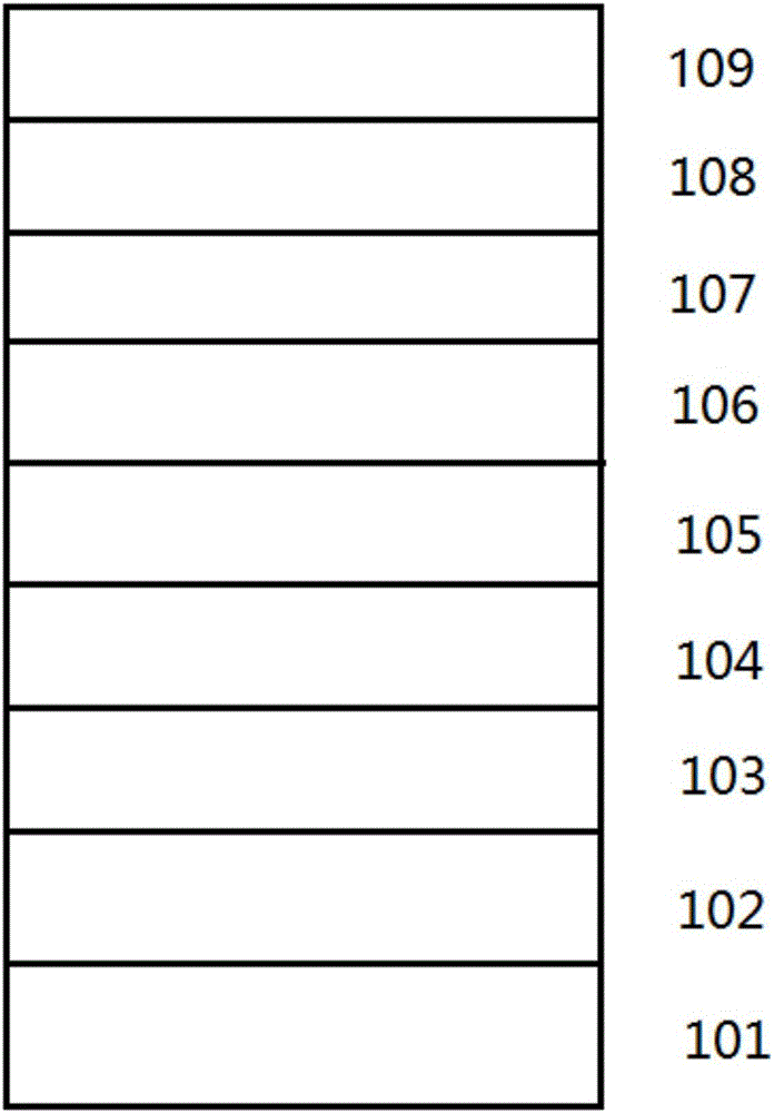
[0024] In the metal organic compound vapor phase epitaxy reaction chamber, the patterned sapphire substrate 101 will be heated in hydrogen (H 2 ) atmosphere, 1080°C-1100°C, reaction chamber pressure 100torr, treatment for 5-15 minutes; then lower the temperature, at 500-550°C, reaction chamber pressure 600torr, H 2 Under the atmosphere, the V / III molar ratio is 100-1500; three-dimensionally grow a 20 nm-thick low-temperature GaN nucleation layer 102;

[0025] At 1000-1100°C, the reaction chamber pressure is 200-300torr, H 2 Under the atmosphere, the V / III molar ratio is 1000-1300; grow a high-temperature non-doped GaN buffer layer 103 with...

Embodiment 2

[0034] Using Aixtron’s close-coupled vertical reaction chamber MOCVD growth system, trimethylgallium (TMGa) or triethylgallium, trimethylaluminum, trimethylindium and ammonia were used as Ga, Al and In during the growth process. and N source, silane (SiH 4 ) as an n-type dopant source, dimagnesocene (Cp 2 Mg) as a p-type dopant source;

[0035] In the metal organic compound vapor phase epitaxy reaction chamber, the patterned sapphire substrate 101 will be 2 ) atmosphere, 1080°C-1100°C, reaction chamber pressure 100torr, treatment for 5-15 minutes; then lower the temperature, at 500-550°C, reaction chamber pressure 600torr, H 2 Under the atmosphere, the V / III molar ratio is 100-1500; three-dimensionally growing a 30 nm-thick low-temperature GaN nucleation layer 102;

[0036] At 1000-1100°C, the reaction chamber pressure is 200-300torr, H 2 Under the atmosphere, the V / III molar ratio is 1000-1300; grow a high-temperature non-doped GaN buffer layer 103 with a thickness of 2 m...


PUM


Abstract

The invention provides a near-ultraviolet LED lamp with a novel electron blocking layer, and a preparation method thereof. A near-ultraviolet LED epitaxial wafer structure comprises a graphical sapphire substrate, a low-temperature GaN nucleating layer, a high-temperature non-doped GaN buffer layer, an n-type GaN layer, an InGaN/AlGaN multiple-quantum well active layer, a p-type AlGaN/InGaN superlattice electron blocking layer, a low-temperature lightly-doped p-type AlInGaN hole expansion layer, a high-temperature p-type GaN layer and a p-type InGaN contact layer. The electron blocking layer adopts a p-type Al<y1>Ga<1 y1>N/In<x1>Ga<1 x1>N superlattice structure. Along with the increase of the number of superlattice periods, the InGaN thickness is reduced step by step, the Mg doping concentration is increased step by step and the hole concentration is increased. By the invention, the hole injection efficiency is effectively improved and the electron hole recombination luminous efficiency is enhanced, so the near-ultraviolet LED luminous efficiency is increased.

Description

technical field [0001] The invention relates to the technical field of semiconductor optoelectronics, a near-ultraviolet light-emitting diode and a preparation method thereof, in particular to a novel electron blocking layer (i.e., a p-type AlGaN / InGaN electron blocking layer) having a stepwise change in its doping concentration and Al composition. ) near-ultraviolet LED and a preparation method thereof. Background technique [0002] Ultraviolet semiconductor light sources are mainly used in biomedicine, anti-counterfeiting identification, purification (water, air, etc.), computer data storage, and military affairs. With the advancement of ultraviolet light technology, new applications will continue to appear to replace the original technology and products, and ultraviolet light LEDs have broad market application prospects. The ultraviolet light source will be developed for general lighting, optical tweezers, plant growth, oil pipeline leak detection, archaeological applica...

Claims


Application Information

Patent Timeline
Patent Type & Authority Applications(China)
IPC IPC(8): H01L33/14H01L33/00B82Y30/00B82Y40/00
CPCB82Y30/00B82Y40/00H01L33/007H01L33/14
Inventor 贾传宇殷淑仪张国义
Owner 东莞市中晶半导体科技有限公司
Why Eureka
Try Eureka