Composite insulating layer for thin film sensor and preparation method of composite insulating layer
A thin-film sensor and composite insulation technology, which is applied in the coating, instrument, superimposed layer plating, etc., can solve the problems of high energy of metal atoms, affecting the compactness of the thin-film insulating layer, and the failure of thin-film sensors
- Summary
- Abstract
- Description
- Claims
- Application Information
AI Technical Summary
Problems solved by technology
Method used
Image
Examples
preparation example Construction
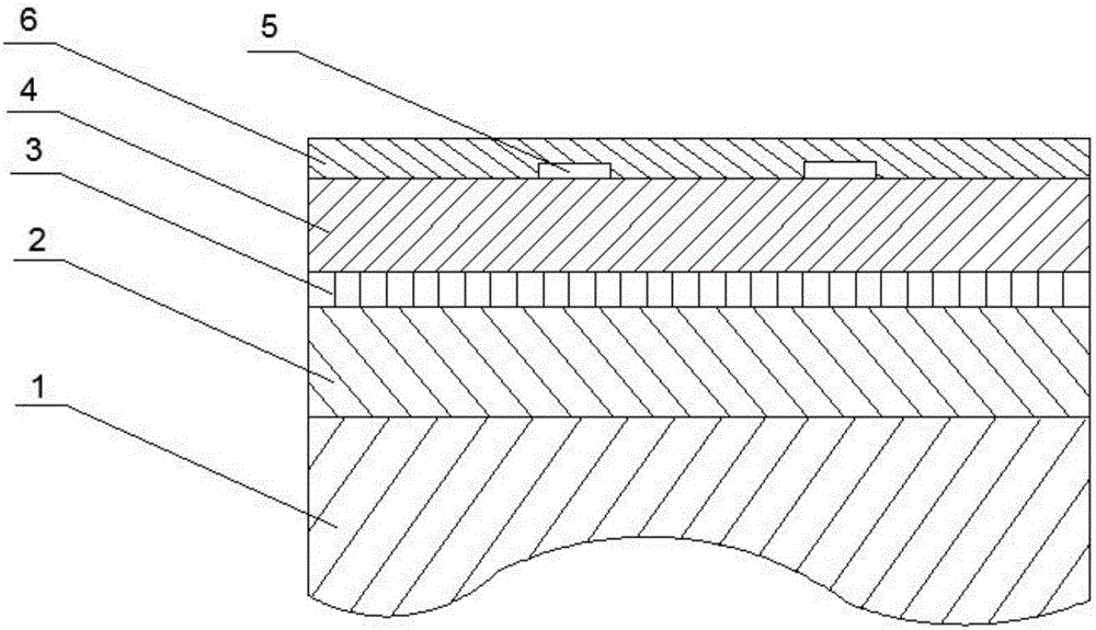
[0038] A method for preparing a film sensor based on a composite insulating layer provided by the invention, specifically comprising the following steps:
[0039]Step 1. Surface treatment of the alloy substrate: first, polish the alloy substrate, then use acetone, ethanol and deionized water to clean the surface of the alloy substrate in turn, and dry it with nitrogen after cleaning;
[0040] Step 2, depositing a NiCrAlY alloy transition layer on the alloy substrate: using DC sputtering to deposit the NiCrAlY alloy on the alloy substrate treated in step 1 to obtain a composite substrate with a NiCrAlY alloy transition layer;
[0041] Step 3, Al 2 o 3 Preparation of thermally grown layer: place the composite substrate obtained after step 2 in a vacuum heat treatment furnace, -3 Aluminum precipitation treatment in a vacuum environment below Pa and a temperature of 800-1200°C for 1-10 hours; then, maintain a temperature of 800-1200°C and feed oxygen to normal pressure, perform ...
Embodiment
[0049] With the nickel-based alloy plate as the alloy substrate to be tested, the process of preparing the S-type thin-film thermocouple with the composite insulating layer of the present invention thereon specifically includes the following steps:
[0050] Step 1. Surface treatment of the alloy substrate: first, polish the surface of the nickel-based alloy substrate with a size of 70mm×15mm×2mm, and then use industrial degreaser, acetone, ethanol, and deionized water to soak the nickel-based alloy substrate successively and ultrasonically Clean for 15 minutes each, after cleaning, dry the surface with dry nitrogen and dry it at 150°C for later use;
[0051] Step 2. Preparation of NiCrAlY alloy transition layer: place the nickel-based alloy substrate cleaned in step 1 on the back with a vacuum degree of 5.0×10 -3 In the vacuum environment of Pa, argon gas with a purity of 99.999% (volume percentage) is introduced as the sputtering medium, and the NiCrAlY alloy is used as the t...
PUM
| Property | Measurement | Unit |
|---|---|---|
| thickness | aaaaa | aaaaa |
| thickness | aaaaa | aaaaa |
| thickness | aaaaa | aaaaa |
Abstract
Description
Claims
Application Information


